ICGOO在线商城 > DG302ACWE+

 Datasheet下载
- 型号: DG302ACWE+
- 制造商: Maxim
- 库位|库存: xxxx|xxxx
- 要求:
| 数量阶梯 | 香港交货 | 国内含税 |
| +xxxx | $xxxx | ¥xxxx |
查看当月历史价格
查看今年历史价格
DG302ACWE+产品简介:
ICGOO电子元器件商城为您提供DG302ACWE+由Maxim设计生产,在icgoo商城现货销售,并且可以通过原厂、代理商等渠道进行代购。 提供DG302ACWE+价格参考以及MaximDG302ACWE+封装/规格参数等产品信息。 你可以下载DG302ACWE+参考资料、Datasheet数据手册功能说明书, 资料中有DG302ACWE+详细功能的应用电路图电压和使用方法及教程。
| 参数 | 数值 |
| 产品目录 | 集成电路 (IC)半导体 |
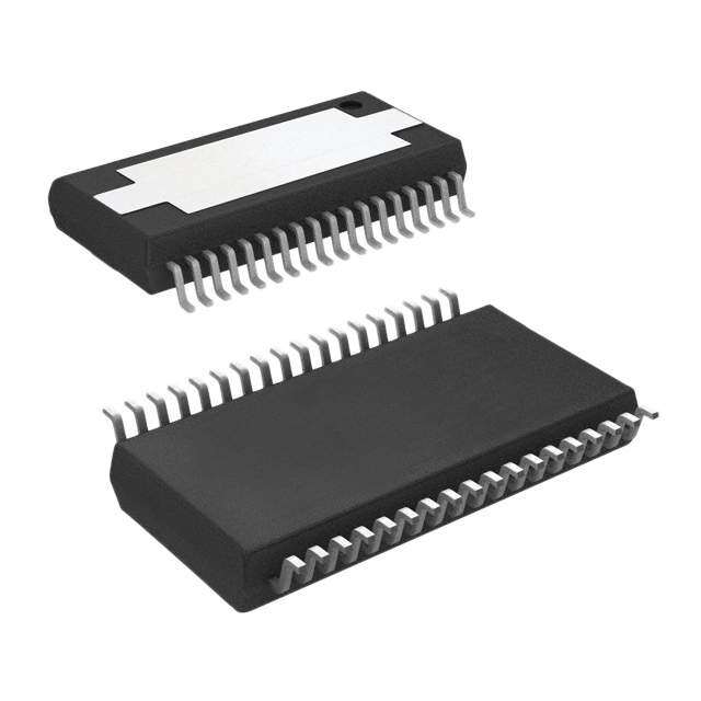
| 描述 | IC SWITCH DUAL DPST 16SOIC模拟开关 IC DUAL DPST CMOS Normally Closed |
| 产品分类 | |
| 品牌 | Maxim Integrated |
| 产品手册 | |
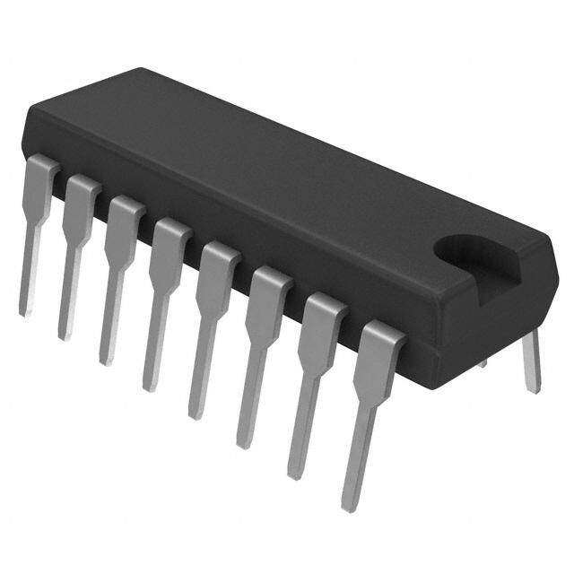
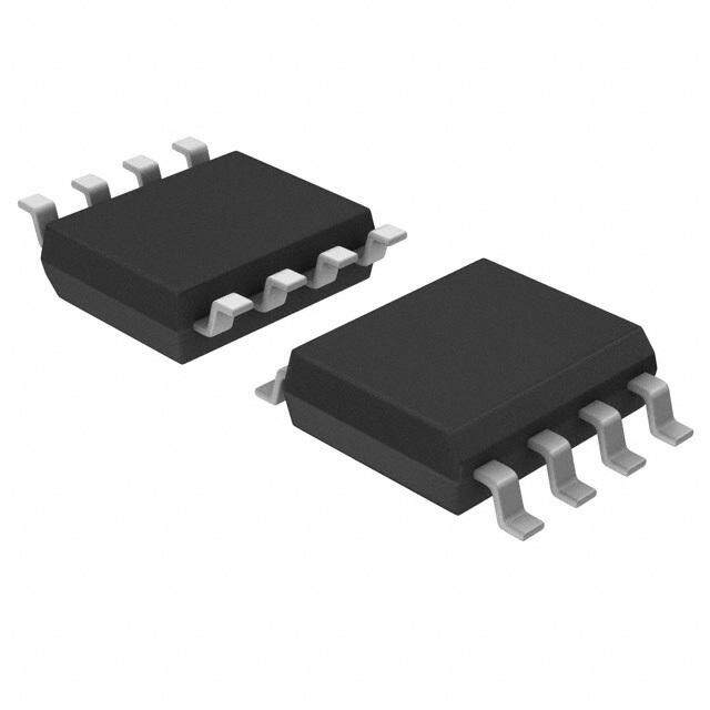
| 产品图片 |
|
| rohs | 符合RoHS无铅 / 符合限制有害物质指令(RoHS)规范要求 |
| 产品系列 | 开关 IC,模拟开关 IC,Maxim Integrated DG302ACWE+- |
| 数据手册 | |
| 产品型号 | DG302ACWE+ |
| 产品培训模块 | http://www.digikey.cn/PTM/IndividualPTM.page?site=cn&lang=zhs&ptm=25703http://www.digikey.cn/PTM/IndividualPTM.page?site=cn&lang=zhs&ptm=25705 |
| 产品种类 | 模拟开关 IC |
| 供应商器件封装 | 16-SOIC W |
| 功能 | |
| 包装 | 管件 |
| 商标 | Maxim Integrated |
| 安装类型 | 表面贴装 |
| 安装风格 | SMD/SMT |
| 导通电阻 | 50 欧姆 |
| 导通电阻—最大值 | 63 Ohms |
| 封装 | Tube |
| 封装/外壳 | 16-SOIC(0.295",7.50mm 宽) |
| 封装/箱体 | SOIC-Wide-16 |
| 工作温度 | 0°C ~ 70°C |
| 工作电源电压 | 0.8 V, 4 V |
| 工厂包装数量 | 46 |
| 开关数量 | 2 |
| 开关电压—最大值 | 15 V |
| 开关配置 | DPST |
| 最大功率耗散 | 450 mW |
| 最大双重电源电压 | +/- 18 V |
| 最大工作温度 | + 70 C |
| 最小工作温度 | 0 C |
| 标准包装 | 46 |
| 电压-电源,单/双 (±) | ±5 V ~ 18 V |
| 电压源 | 双电源 |
| 电流-电源 | 230µA |
| 电源电压-最大 | 44 V |
| 电源电压-最小 | 0.8 V, 4 V |
| 电源电流 | 0.001 uA |
| 电源电流—最大值 | 10 uA |
| 电路 | 2 x DPST - NO |
| 空闲时间—最大值 | 250 ns |
| 系列 | DG302A |
| 运行时间—最大值 | 300 ns |
| 零件号别名 | DG302A |










PDF Datasheet 数据手册内容提取
19-0309; Rev 3; 11/07 TTL Compatible CMOS Analog Switches General Description Features D Maxim’s DG300–DG303 and DG300A–DG303A CMOS ♦ Monolithic Low-Power CMOS G dual and quad analog switches combine low power operation with fast switching times and superior DC and ♦ Latchup Proof Construction 3 0 AC switch characteristics. On-resistance is less than ♦ Fully Compatible 2nd Source 50Ω and is essentially constant over the analog signal 0 range. Device specifications are ideal for battery- ♦ Low On-Resistance, <50Ω ( powered circuitry. ♦ Fast Switching Time A These switches are available in a variety of formats as ) ♦ V+ to V- Analog Signal Range / outlined in the Pin Configurations section. The switch D control logic inputs are fully TTL and CMOS compati- ♦ Single-Supply Capability G ble. Also featured are “break-before-make” switching and low charge injection. 3 Ordering Information 0 Maxim’s DG300-DG303 and DG300A-DG303A families are electrically compatible and pin compatible with the 1 PART TEMP RANGE PIN-PACKAGE original manufacturer’s devices. All devices operate with ( power supplies ranging from ±5V to ±18V. Single-sup- DG300C/D 0°C to +70°C Dice A ply operation is implemented by connecting V- to GND. DG300CJ 0°C to +70°C 14 Lead Plastic DIP ) / Applications DG300CWE 0°C to +70°C 16 Lead Wide SO D DG300CK 0°C to +70°C 14 Lead CERDIP G Portable Instruments DG300BWE -25°C to +85°C 16 Lead Wide SO 3 Low-Power Sample/Holds DG300BK -25°C to +85°C 14 Lead CERDIP 0 Power-Supply Switching DG300BA -25°C to +85°C 10 Lead Metal Can 2 Programmable Gain Amplifiers DG300AK -55°C to +125°C 14 Lead CERDIP ( A SPDT and DPDT Functions DG300AA -55°C to +125°C 10 Lead Metal Can Process Control and Telemetry Ordering Information continued at end of data sheet. ) / D Pin Configurations G 3 DUAL SPST DG300/DG300A DUAL DPST DG302/DG302A V+ (SUBSTRATE AND CASE) 0 N.C. 1 14V+ N.C. 1 14V+ D11 10 9 D2 D1 2 13D2 S3 2 13S4 3 S1 2 8 S2 N.C. 3 12N.C. D3 3 12D4 ( S1 4 11S2 D1 4 11D2 A IN1 3 7 IN2 N.C. 5 10N.C. S1 5 10S2 N.C.4 5 6 V- IN1 6 9 IN2 IN1 6 9 IN2 ) GND GND 7 8 V- GND 7 8 V- LOGICSWITCH LOGIC SWITCH 0 OFF 0 OFF 1 ON 1 ON SPDT DG301/DG301A DUAL SPDT DG303/DG303A V+ (SUBSTRATE AND CASE) N.C. 1 14V+ N.C. 1 14V+ D11 10 9 D2 D1 2 13D2 S3 2 13S4 S1 2 8 S2 N.C. 3 12N.C. D3 3 12D4 S1 4 11S2 D1 4 11D2 IN 3 7 N.C. N.C. 5 10N.C. S1 5 10S2 N.C.4 5 6 V- IN 6 9 N.C. IN1 6 9 IN2 GND GND 7 8 V- GND 7 8 V- LOGICSWITCH 1SWITCH 2 LOGIC SWITCHES 1, 2 SWITCHES 3, 4 0 OFF ON 0 OFF ON 1 ON OFF 1 ON OFF SWITCH STATES ARE FOR LOGIC "1" INPUTS (POSITIVE LOGIC). ________________________________________________________________Maxim Integrated Products 1 For pricing, delivery, and ordering information,please contact Maxim Direct at 1-888-629-4642, or visit Maxim’s website at www.maxim-ic.com.
TTL Compatible CMOS Analog Switches ) ABSOLUTE MAXIMUM RATINGS A Voltages Referenced to V- Operating Temperature (A suffix)......................-55°C to +125°C ( V+ (DG300–DG303)...............................................................36V (B suffix)........................-25°C to +85°C 3 V+ (DG300A–DG303A)..........................................................44V (C suffix)...........................0°C to +70°C 0 GND.......................................................................................25V Lead Temperature (soldering 10s)..................................+300°C 3 Digital Inputs, VS, VD, (Note 1).......................-4V to (V+ + 4V) or Power Dissipation* 30mA, whichever occurs first Cerdip (K) (derate 11mW/°C above +75°C)....................825mW G Current, Any Terminal Except S or D..................................30mA Plastic DIP (J) (derate 6.5mW/°C above +25°C).............470mW D Continuous Current, S or D.................................................30mA Metal Can (A) (derate 6mW/°C above +75°C).................450mW (pulsed at 1ms, 10% duty cycle max)..........................100mA )/ Storage Temperature (A & B suffix)...................-65°C to +150°C *Device mounted with all leads soldered or welded to PC board. A (C suffix).........................-65°C to +125°C ( 2 Stresses beyond those listed under “Absolute Maximum Ratings” may cause permanent damage to the device. These are stress ratings only, and functional operation of the device at these or any other conditions beyond those indicated in the operational sections of the specifications is not implied. Exposure to 0 absolute maximum rating conditions for extended periods may affect device reliability. 3 G ELECTRICAL CHARACTERISTICS D (V+ = +15V, V- = -15V, GND = 0V, TA= +25°C, unless otherwise noted.) / DG300–DG303A DG300–DG303B/C ) A DG300A–DG303AA DG300A–DG303AB/C PARAMETER SYMBOL TEST CONDITIONS UNITS MIN TYP MAX MIN TYP MAX ( 1 (Note 2) (Note 3) (Note 2) (Note 3) 0 Analog Signal Range VANALOG IS = 10mA, VIN = 0.8V or 4.0V -15 +15 -15 +15 V 3 Drain-Source RDS(ON) IS = -10mA, VD = 10V 30 50 30 50 Ω ON-Resistance IS = -10mA, VD = -10V 30 50 30 50 G D WITCH SLeoaukrcaeg eO CFFu-rrent IS(OFF) VIN =o r0.8V VVSS == 1-144VV, ,V VDD = = - 1144VV -1 -00..11 1 -5 -00..11 5 nA )/ S Drain OFF- ID(OFF) VIN = 0.8V VS = -14V, VD = 14V 0.1 1 0.1 5 nA A Leakage Current VS = 14V, VD = -14V -1 -0.1 -5 -0.1 Drain ON- VD = VS = 14V 0.1 2 0.1 5 ( ID(ON) nA 0 Leakage Current VD = VS = -14V -2 -0.1 -5 -0.1 0 T Input Current/ IINH VIN = 5.0V -1 -0.001 -1 -0.001 µA U Voltage High VIN = 15V 0.001 1 0.001 1 3 P N Input Current/ G I IINL VIN = 0V -1 -0.001 -1 -0.001 µA Voltage Low D Turn-ON Time tON 150 300 150 300 ns See Switching Time Test Circuit Turn-OFF Time tOFF 130 250 130 250 ns Break-Before-Make See Break-Before-Make Time Test tON - tOFF 50 50 ns Interval Circuit, DG301(A)/DG303(A) only Charge Injection Q CL = 10nF, RGEN = 0Ω, VGEN = 0V 12 12 pC Source OFF- CS(OFF) VS = 0V 14 14 pF C Capacitance f = 1MHz, AMI Drain OFF- CD(OFF) VIN = 0.8V VD = 0V 14 14 pF N Capacitance or Y D Channel ON- CD(ON) + VIN = 4.0V VS = VD = 0V 40 40 pF Capacitance CS(ON) VIN = 0V 6 6 Input Capacitance CIN f = 1MHz pF VIN = 15V 7 7 Off-Isolation (Note 4) 62 62 dB VIN = 0V, RL = 1kΩ Crosstalk VS = 1VRMS, f = 500kHz 74 74 dB (Channel-to-Channel) 2 _______________________________________________________________________________________
TTL Compatible CMOS Analog Switches ELECTRICAL CHARACTERISTICS (continued) D (V+ = +15V, V- = -15V, GND = 0V, TA= +25°C, unless otherwise noted.) G DG300–DG303A DG300–DG303B/C 3 PARAMETER SYMBOL TEST CONDITIONS DG300A–DG303AA DG300A–DG303AB/C UNITS 0 MIN TYP MAX MIN TYP MAX 0 (Note 2) (Note 3) (Note 2) (Note 3) ( Positive Supply I+ 0.23 0.5 0.23 0.5 mA A Current VIN = 4V (one input) ) Y Negative Supply I- (all others = 0) -10 -0.001 -10 -0.001 µA / PL Current D UP Positive Supply I+ 0.001 10 0.001 10 µA G S Current VIN = 0.8V (all inputs) 3 Negative Supply I- -10 -0.001 -10 -0.001 µA 0 Current 1 ELECTRICAL CHARACTERISTICS (Over Temperature) ( A (V+ = +15V, V- = -15V, GND = 0V, TA= Over Temperature Range, unless otherwise noted.) ) DG300–DG303A DG300–DG303B/C / DG300A–DG303AA DG300A–DG303AB/C D PARAMETER SYMBOL TEST CONDITIONS UNITS MIN TYP MAX MIN TYP MAX G (Note 2) (Note 3) (Note 2) (Note 3) 3 Analog Signal Range VANALOG IS = -10mA, VIN = 0.8V or 4.0V -15 +15 -15 +15 V 0 DOrNa-inR-eSsoisutracnece RDS(ON) IISS == --1100mmAA,, VVDD == 1-100VV 7755 7755 Ω 2 WITCH SLeoaukrcaeg eO CFFu-rrent IS(OFF) VIN =o r0.8V VVSS == 1-144VV, ,V VDD = = - 1144VV -100 100 -100 100 nA (A S Drain OFF- ID(OFF) VIN = 0.8V VS = -14V, VD = 14V 100 100 nA )/ Leakage Current VS = 14V, VD = -14V -100 -100 D Drain ON- ID(ON) VD = VS = 14V 200 200 nA G Leakage Current VD = VS = -14V -200 -200 Input Current/ VIN = 5.0V -1 -10 3 UT Voltage High IINH VIN = 15V 1 10 µA 0 P N Input Current/ 3 I IINL VIN = 0V -1 -10 µA Voltage Low ( Positive Supply A I+ 1 1 mA Current VIN = 4V (one input) ) Y Negative Supply I- (all others = 0) -100 -200 mA PL Current P U Positive Supply I+ 100 200 µA S Current VIN = 0.8V (all inputs) Negative Supply I- -100 -200 µA Current MIC Turn-ON Time tON 500 ns A See Switching Time Test Circuit N DY Turn-OFF Time tOFF 450 ns _______________________________________________________________________________________ 3
TTL Compatible CMOS Analog Switches ) ELECTRICAL CHARACTERISTICS (Over Temperature) (continued) A (V+ = +15V, V- = -15V, GND = 0V, TA= Over Temperature Range, unless otherwise noted.) ( 3 0 Note 1: Signals on SX, DX, or INXexceeding V+ or V- are clamped by internal diodes. Limit diode forward current to maximum cur- rent ratings. 3 Note 2: The algebraic convention whereby the most negative value is a minimum, and the most positive value is a maximum is used G in this data sheet. D Note 3: Typical values are for DESIGNAIDONLY, not guaranteed nor subject to production testing. )/ Note 4: OFF-isolation = 20 log VVDS , VS= input to OFF switch, VD= output. A Typical Operating Characteristics ( 2 (TA= +25°C, unless otherwise noted.) 0 3 G D / ) A ( 1 0 3 G D / ) A ( 0 0 3 G D 4 _______________________________________________________________________________________
TTL Compatible CMOS Analog Switches Test Circuits D G ΔVO 3 0 0 RGEN SX DX VO VO (A CL VGEN 10nF ) / INX +4V D INX ON ON G OFF 3 0V 0 ΔVO = Δ MEASURED VOLTAGE ERROR DUE TO CHARGE INJECTION 1 THE ERROR VOLTAGE IN COULOMBS IS ΔQ = CL x ΔVO. ( Figure 1. Charge Injection Test Circuit A ) / LOGIC "1" = SWITCH ON D LOGIC VIHN +15V G INPUT 50% +4V V+ SWITCH 0V VS1 = 3VS1 D1 OUTPUVTO1 30 VS1 S2 D2 VS2 = 3V VO2 2 SWITCH IN RL2 RL1 CL2 CL1 ( OUTPUT 50% 300Ω 300Ω 33pF 33pF A VO1 0V ) GND V- LOGIC / VS2 INPUT -15V D VO2 G SWITCH 50% OUTPUT 3 0V 0 tBBM 3 Figure 2. Break-Before-Make Time Test Circuit SPDT (DG301(A), DG303(A) ( A ) LOGIC "1" = SWITCH ON +15V LOGIC VIHN V+ INPUT 50% +4V SWITCH ttRF << 2200nnss 0V S 0 OUTPUT VS = 3V VO IN RL CL VS 300Ω 33pF SWITCH OUTPUT 90% GND V- LOGIC 10% INPUT -15V 0V tON tOFF Figure 3. Switching Time Test Circuit _______________________________________________________________________________________ 5
TTL Compatible CMOS Analog Switches ) Table 1. Typical Single Supply Parameters A V+ SUPPLY VOLTAGE (V- = 0V) ( PARAMETER 3 +10V +15V +20V +30V 0 3 Switching Time (RL = 1kΩ) tON 190ns 150ns 110ns 70ns tOFF 40ns 40ns 40ns 40ns G VSIGNAL = +1V 71Ω 51Ω 42Ω 31Ω D On-Resistance VSIGNAL = V+ / 2 77Ω 54Ω 43Ω 30Ω / VSIGNAL = V+ 84Ω 63Ω 54Ω 43Ω ) A Input Logic Levels 0.8V, 4.0V 0.8V, 4.0V 0.8V, 4.0V 0.8V, 4.5V ( 2 Applications Information Table 2. Charge Injection (±15V Supplies) 0 All DG300 family switches will operate with ±5V to ±15V ANALOG INPUT (V) INJECTED Q (pC) 3 power supplies. They can also be used with single-ended +10 4 G power supplies ranging from +10V to +30V where the V- +5 8 terminal is connected to ground. In either case, analog D signals ranging from V+ to V- can be switched. 0 12 )/ The on-resistance variation with analog signal and supply -5 8 A voltage is shown in the Typical Operating Characteristics. -10 5 ( The temperature coefficient of RONis typically 0.5%/°C. 1 Typical on-resistance matching from channel to chan- The charge injection test circuit is shown in Figure 1. 0 nel is 10%. In addition, Table 1 outlines some typical Table 2 lists the typical injected charge for DG300 series 3 parameters for single-supply operation. switches with various input voltages. G D / Chip Topography ) A ( b a n m DIE PAD DG300 DG301 DG302/DG303 0 DG300A DG301A DG302A/DG303A a N.C. N.C. S3 0 l b D1 D1 D3 3 c N.C. S1 D1 G d S1 N.C. S1 D e IN1 IN1 IN1 c k f N.C. N.C. N.C. 0.106" g GND GND GND 2.69mm h V- V- V- d j i IN2 N.C. IN2 j S2 N.C. S2 k N.C. N.C. D2 l D2 S2 D4 m N.C. D2 S4 e f g h i n V+ V+ V+ 0.108" 2.74mm 6 _______________________________________________________________________________________
TTL Compatible CMOS Analog Switches Ordering Information (continued) D G PART TEMP RANGE PIN-PACKAGE PART TEMP RANGE PIN-PACKAGE 3 DG300AC/D 0°C to +70°C Dice DG302CWE 0°C to +70°C 16 Lead Wide SO 0 DG300ACJ 0°C to +70°C 14 Lead Plastic DIP DG302CK 0°C to +70°C 14 Lead CERDIP 0 DG300ACWE 0°C to +70°C 16 Lead Wide SO DG302BWE -25°C to +85°C 16 Lead Wide SO ( DG300ACK 0°C to +70°C 14 Lead CERDIP DG302BK -25°C to +85°C 14 Lead CERDIP A DG300ABWE -25°C to +85°C 16 Lead Wide SO DG302AK -55°C to +125°C 14 Lead CERDIP ) DG300ABK -25°C to +85°C 14 Lead CERDIP DG302AC/D 0°C to +70°C Dice / D DG300ABA -25°C to +85°C 10 Lead Metal Can DG302ACJ 0°C to +70°C 14 Lead Plastic DIP G DG301C/D 0°C to +70°C Dice DG302ACWE 0°C to +70°C 16 Lead Wide SO 3 DG301CJ 0°C to +70°C 14 Lead Plastic DIP DG302ACK 0°C to +70°C 14 Lead CERDIP 0 DG301CWE 0°C to +70°C 16 Lead Wide SO DG302ABWE -25°C to +85°C 16 Lead Wide SO 1 DG301CK 0°C to +70°C 14 Lead CERDIP DG302ABK -25°C to +85°C 14 Lead CERDIP ( DG301BWE -25°C to +85°C 16 Lead Wide SO DG303C/D 0°C to +70°C Dice A DG301BK -25°C to +85°C 14 Lead CERDIP DG303CJ 0°C to +70°C 14 Lead Plastic DIP ) / DG301BA -25°C to +85°C 10 Lead Metal Can DG303CWE 0°C to +70°C 16 Lead Wide SO D DG301AK -55°C to +125°C 14 Lead CERDIP DG303CK 0°C to +70°C 14 Lead CERDIP G DG301AA -55°C to +125°C 10 Lead Metal Can DG303BWE -25°C to +85°C 16 Lead Wide SO 3 DG301AC/D 0°C to +70°C Dice DG303BK -25°C to +85°C 14 Lead CERDIP 0 DG301ACJ 0°C to +70°C 14 Lead Plastic DIP DG303AK -55°C to +125°C 14 Lead CERDIP 2 DG301ACWE 0°C to +70°C 16 Lead Wide SO DG303AC/D 0°C to +70°C Dice ( DG301ACK 0°C to +70°C 14 Lead CERDIP DG303ACJ 0°C to +70°C 14 Lead Plastic DIP A DG301ABWE -25°C to +85°C 16 Lead Wide SO DG303ACWE 0°C to +70°C 16 Lead Wide SO ) / DG301ABK -25°C to +85°C 14 Lead CERDIP DG303ACK 0°C to +70°C 14 Lead CERDIP D DG301ABA -25°C to +85°C 10 Lead Metal Can DG303ABWE -25°C to +85°C 16 Lead Wide SO G DG302C/D 0°C to +70°C Dice DG303ABK -25°C to +85°C 14 Lead CERDIP 3 DG302CJ 0°C to +70°C 14 Lead Plastic DIP 0 3 ( A ) _______________________________________________________________________________________ 7
TTL Compatible CMOS Analog Switches ) Package Information A (The package drawing(s) in this data sheet may not reflect the most current specifications. For the latest package outline information, ( go to www.maxim-ic.com/packages.) 3 0 S 3 P E G PN. DI D P / ) A ( 2 0 3 G D / ) A ( 1 0 3 G D / ) A ( 0 0 3 G D 8 _______________________________________________________________________________________
TTL Compatible CMOS Analog Switches Package Information (continued) D (The package drawing(s) in this data sheet may not reflect the most current specifications. For the latest package outline information, G go to www.maxim-ic.com/packages.) 3 0 S 0 P E W. ( N DIM MIINNCHEMSAX MMIILNLIMETMERASX SOIC A A 0.093 0.104 2.35 2.65 ) A1 0.004 0.012 0.10 0.30 /D B 0.014 0.019 0.35 0.49 C 0.009 0.013 0.23 0.32 G e 0.050 1.27 E H E 0.291 0.299 7.40 7.60 3 H 0.394 0.419 10.00 10.65 0 L 0.016 0.050 0.40 1.27 1 VARIATIONS: ( 1 A INCHES MILLIMETERS TOP VIEW DIM MIN MAX MIN MAX N MS013 ) / D 0.398 0.413 10.10 10.50 16 AA D D 0.447 0.463 11.35 11.75 18 AB D 0.496 0.512 12.60 13.00 20 AC G D 0.598 0.614 15.20 15.60 24 AD D D 0.697 0.713 17.70 18.10 28 AE 3 0 2 A C ( A e B A1 0∞-8∞ ) FRONT VIEW L / D SIDE VIEW G 3 0 PROPRIETARY INFORMATION TITLE: 3 PACKAGE OUTLINE, .300" SOIC ( APPROVAL DOCUMENT CONTROL NO. REV. 1 21-0042 B 1 A ) _______________________________________________________________________________________ 9
TTL Compatible CMOS Analog Switches ) Package Information (continued) A (The package drawing(s) in this data sheet may not reflect the most current specifications. For the latest package outline information, ( go to www.maxim-ic.com/packages.) 3 0 G3 CDIPS.EPS D / ) A ( 2 0 3 G D / ) A ( 1 0 3 G D / ) A ( 0 0 3 G D 10 ______________________________________________________________________________________
TTL Compatible CMOS Analog Switches Revision History D G REVISION REVISION PAGES DESCRIPTION NUMBER DATE CHANGED 3 0 0 2/88 Initial release — 0 1 6/99 Errors in the test limits and pin configuration — ( 2 9/04 Fixed Truth Table — A 3 11/07 Correction to pin configuration 1 ) / D G 3 0 1 ( A ) / D G 3 0 2 ( A ) / D G 3 0 3 ( A ) Maxim cannot assume responsibility for use of any circuitry other than circuitry entirely embodied in a Maxim product. No circuit patent licenses are implied. Maxim reserves the right to change the circuitry and specifications without notice at any time. Maxim Integrated Products, 120 San Gabriel Drive, Sunnyvale, CA 94086 408-737-7600 ____________________11 © 2007 Maxim Integrated Products is a registered trademark of Maxim Integrated Products, Inc.
Mouser Electronics Authorized Distributor Click to View Pricing, Inventory, Delivery & Lifecycle Information: M axim Integrated: DG301AAK/883B DG302AAK/883B DG303AAK/883B DG300ACJ+ DG303ACWE+ DG300ABWE+ DG300ABWE+T DG300ACWE+ DG300ACWE+T DG301ACJ+ DG301ACWE+ DG301ACWE+T DG302ACJ+ DG302ACWE+ DG302ACWE+T DG303ACJ+ DG303ACWE+T DG303AEWE+ DG303AEWE+T DG302ABK DG303AC/D DG300AAK/883B DG303ABK DG303ABWE+