ICGOO在线商城 > DS1315EN-33+

 Datasheet下载
- 型号: DS1315EN-33+
- 制造商: Maxim
- 库位|库存: xxxx|xxxx
- 要求:
| 数量阶梯 | 香港交货 | 国内含税 |
| +xxxx | $xxxx | ¥xxxx |
查看当月历史价格
查看今年历史价格
DS1315EN-33+产品简介:
ICGOO电子元器件商城为您提供DS1315EN-33+由Maxim设计生产,在icgoo商城现货销售,并且可以通过原厂、代理商等渠道进行代购。 提供DS1315EN-33+价格参考以及MaximDS1315EN-33+封装/规格参数等产品信息。 你可以下载DS1315EN-33+参考资料、Datasheet数据手册功能说明书, 资料中有DS1315EN-33+详细功能的应用电路图电压和使用方法及教程。
| 参数 | 数值 |
| 产品目录 | 集成电路 (IC)半导体 |
| 描述 | IC RTC PHANTOM PAR 20-TSSOP实时时钟 Phantom Time Chip |
| 产品分类 | |
| 品牌 | Maxim Integrated |
| 产品手册 | |
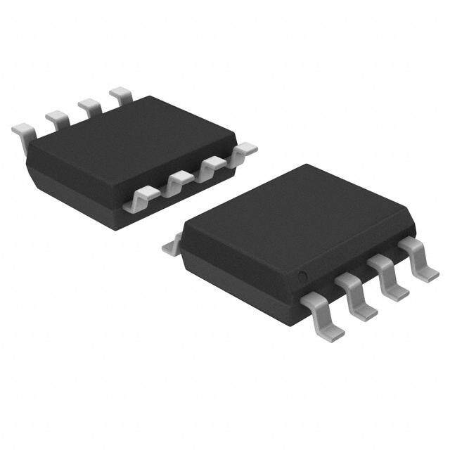
| 产品图片 |
|
| rohs | 符合RoHS无铅 / 符合限制有害物质指令(RoHS)规范要求 |
| 产品系列 | 时钟和计时器IC,实时时钟,Maxim Integrated DS1315EN-33+- |
| 数据手册 | |
| 产品型号 | DS1315EN-33+ |
| 产品培训模块 | http://www.digikey.cn/PTM/IndividualPTM.page?site=cn&lang=zhs&ptm=25703http://www.digikey.cn/PTM/IndividualPTM.page?site=cn&lang=zhs&ptm=25705 |
| 产品种类 | 实时时钟 |
| 供应商器件封装 | 20-TSSOP |
| 功能 | Clock, Calendar |
| 包装 | 管件 |
| 商标 | Maxim Integrated |
| 存储容量 | - |
| 安装类型 | 表面贴装 |
| 安装风格 | SMD/SMT |
| 封装 | Tube |
| 封装/外壳 | 20-TSSOP(0.173",4.40mm 宽) |
| 封装/箱体 | TSSOP-20 |
| 工作温度 | -40°C ~ 85°C |
| 工厂包装数量 | 74 |
| 应用说明 | 点击此处下载产品Datasheet点击此处下载产品Datasheet点击此处下载产品Datasheet点击此处下载产品Datasheet点击此处下载产品Datasheet点击此处下载产品Datasheet点击此处下载产品Datasheet点击此处下载产品Datasheet点击此处下载产品Datasheet |
| 接口 | 并联 |
| 日期格式 | YY-MM-DD-dd |
| 时间格式 | HH:MM:SS:hh(12/24 小时) |
| 最大工作温度 | + 85 C |
| 最小工作温度 | - 40 C |
| 标准包装 | 1 |
| 特性 | 闰年 |
| 电压-电源 | 3 V ~ 3.6 V |
| 电压-电源,电池 | 2.5 V ~ 3.7 V |
| 电池备用开关 | Yes |
| 电流-计时(最大) | 1.1mA @ 3.3V |
| 电源电压-最大 | 3.6 V |
| 电源电压-最小 | 3 V |
| 类型 | Phantom 计时芯片 |
| 系列 | DS1315EN |
| 零件号别名 | 90-1315E+N33 DS1315EN |










PDF Datasheet 数据手册内容提取
19-6080; Rev 11/11 www.dalsemi.com DS1315 Phantom Time Chip DESCRIPTION FEATURES The DS1315 Phantom Time Chip is a Real-Time Clock Keeps Track of Hundredths combination of a CMOS timekeeper and a of Seconds, Seconds, Minutes, Hours, Days, nonvolatile memory controller. In the absence of Date of the Month, Months, and Years power, an external battery maintains the Automatic Leap Year Correction Valid Up to timekeeping operation and provides power for a 2100 CMOS static RAM. The watch keeps track of No Address Space Required to Communicate hundredths of seconds, seconds, minutes, hours, with RTC day, date, month, and year information. The last Provides Nonvolatile Controller Functions for day of the month is automatically adjusted for Battery Backup of SRAM months with fewer than 31 days, including leap Supports Redundant Battery Attachment for year correction. The watch operates in one of two High-Reliability Applications formats: a 12-hour mode with an AM/PM Full ±10% V Operating Range CC indicator or a 24-hour mode. The nonvolatile +3.3V or +5V Operation controller supplies all the necessary support Industrial (-40°C to +85°C) Operating circuitry to convert a CMOS RAM to a Temperature Ranges Available nonvolatile memory. The DS1315 can be interfaced with either RAM or ROM without PIN DESCRIPTION leaving gaps in memory. X1, X2 - 32.768kHz Crystal Connection WE - Write Enable PIN CONFIGURATIONS BAT1 - Battery 1 Input GND - Ground D - Data Input X1 1 16 VCC1 Q - Data Output X2 2 DS1315 15 VCC0 ROM/RAM - ROM/RAM Mode Select CEO - Chip Enable Output WE 3 14 BAT2 CEI - Chip Enable Input BAT1 4 13 RST OE - Output Enable GND 5 12 OE RST - Reset D 6 11 CEI BAT2 - Battery 2 Input Q 7 10 CEO VCC0 - Switched Supply Output V - Power Supply Input GND 8 9 ROM/RAM CC1 PDIP (300 mils) Pin Configurations continued at end of data sheet. 1 of 21
DS1315 Phantom Time Chip ORDERING INFORMATION VOLTAGE PART TEMP RANGE PIN-PACKAGE TOP MARK* (V) DS1315-33+ 0°C to +70°C 3.3 16 PDIP (300 mils) DS1315 336 DS1315N-33+ -40°C to +85°C 3.3 16 PDIP (300 mils) DS1315 336 DS1315-5+ 0°C to +70°C 5 16 PDIP (300 mils) DS1315 56 DS1315N-5+ -40°C to +85°C 5 16 PDIP (300 mils) DS1315 56 DS1315E-33+ 0°C to +70°C 3.3 20 TSSOP (4.4mm) DS1315E XXXX-336 DS1315EN-33+ -40°C to +85°C 3.3 20 TSSOP (4.4mm) DS1315E XXXX-336 DS1315EN-33+T&R -40°C to +85°C 3.3 20 TSSOP (4.4mm) DS1315E XXXX-336 DS1315E-5+ 0°C to +70°C 5 20 TSSOP (4.4mm) DS1315E XXXX-56 DS1315EN-5+ -40°C to +85°C 5 20 TSSOP (4.4mm) DS1315E XXXX-56 DS1315EN-5+T&R -40°C to +85°C 5 20 TSSOP (4.4mm) DS1315E XXXX-56 DS1315S-33+ 0°C to +70°C 3.3 16 SO (300 mils) DS1315 336 DS1315SN-33+ -40°C to +85°C 3.3 16 SO (300 mils) DS1315 336 DS1315S-5+ 0°C to +70°C 5 16 SO (300 mils) DS1315 56 DS1315SN-5+ -40°C to +85°C 5 16 SO (300 mils) DS1315S 56 DS1315S-5+T&R 0°C to +70°C 5 16 SO (300 mils) DS1315S 56 +Denotes a lead(Pb)-free/RoHS-compliant package. T&R = Tape and reel. *A “+” symbol located anywhere on the top mark indicates a lead-free device. An “N” located in the bottom right-hand corner of the top of the package denotes an industrial device. “xxxx” can be any combination of characters. 2 of 21
DS1315 Phantom Time Chip Figure 1. Block Diagram 3 of 21
DS1315 Phantom Time Chip Operation Communication with the Time Chip is established by pattern recognition of a serial bit stream of 64 bits which must be matched by executing 64 consecutive write cycles containing the proper data on data in (D). All accesses which occur prior to recognition of the 64-bit pattern are directed to memory via the chip enable output pin (CEO). After recognition is established, the next 64 read or write cycles either extract or update data in the Time Chip and CEO remains high during this time, disabling the connected memory. Data transfer to and from the timekeeping function is accomplished with a serial bit stream under control of chip enable input (CEI), output enable (OE), and write enable (WE). Initially, a read cycle using the CEI and OE control of the Time Chip starts the pattern recognition sequence by moving pointer to the first bit of the 64-bit comparison register. Next, 64 consecutive write cycles are executed using the CEI and WE control of the Time Chip. These 64 write cycles are used only to gain access to the Time Chip. When the first write cycle is executed, it is compared to bit 1 of the 64-bit comparison register. If a match is found, the pointer increments to the next location of the comparison register and awaits the next write cycle. If a match is not found, the pointer does not advance and all subsequent write cycles are ignored. If a read cycle occurs at any time during pattern recognition, the present sequence is aborted and the comparison register pointer is reset. Pattern recognition continues for a total of 64 write cycles as described above until all the bits in the comparison register have been matched. (This bit pattern is shown in Figure 2). With a correct match for 64 bits, the Time Chip is enabled and data transfer to or from the timekeeping registers may proceed. The next 64 cycles will cause the Time Chip to either receive data on D, or transmit data on Q, depending on the level of OE pin or the WE pin. Cycles to other locations outside the memory block can be interleaved with CEI cycles without interrupting the pattern recognition sequence or data transfer sequence to the Time Chip. A standard 32.768kHz quartz crystal can be directly connected to the DS1315 via pins 1 and 2 (X1, X2). The crystal selected for use should have a specified load capacitance (C ) of 6 pF. For more information L on crystal selection and crystal layout considerations, refer to Application Note 58: Crystal Considerations with Maxim Real-Time Clocks (RTCs). 4 of 21
DS1315 Phantom Time Chip Figure 2. Time Chip Comparison Register Definition Note: The pattern recognition in Hex is C5, 3A, A3, 5C, C5, 3A, A3, 5C. The odds of this pattern being accidentally duplicated and causing inadvertent entry to the Phantom Time Chip are less than 1 in 1019. 5 of 21
DS1315 Phantom Time Chip Nonvolatile Controller Operation The operation of the nonvolatile controller circuits within the Time Chip is determined by the level of the ROM/RAM select pin. When ROM/RAM is connected to ground, the controller is set in the RAM mode and performs the circuit functions required to make CMOS RAM and the timekeeping function nonvolatile. A switch is provided to direct power from the battery inputs or V to V with a CCI CCO maximum voltage drop of 0.3 volts. The V output pin is used to supply uninterrupted power to CMOS CCO SRAM. The DS1315 also performs redundant battery control for high reliability. On power-fail, the battery with the highest voltage is automatically switched to V . If only one battery is used in the CCO system, the unused battery input should be connected to ground. The DS1315 safeguards the Time Chip and RAM data by power-fail detection and write protection. Power-fail detection occurs when V falls below V which is set by an internal bandgap reference. The CCI PF DS1315 constantly monitors the V supply pin. When V is less than V , power-fail circuitry forces CCI CCI PF the chip enable output (CEO) to VCCI or VBAT-0.2 volts for external RAM write protection. During nominal supply conditions, CEO will track CEI with a propagation delay. Internally, the DS1315 aborts any data transfer in progress without changing any of the Time Chip registers and prevents future access until V exceeds V . A typical RAM/Time Chip interface is illustrated in Figure 3. CCI PF When the ROM/RAM pin is connected to VCCO, the controller is set in the ROM mode. Since ROM is a read-only device that retains data in the absence of power, battery backup and write protection is not required. As a result, the chip enable logic will force CEO low when power fails. However, the Time Chip does retain the same internal nonvolatility and write protection as described in the RAM mode. A typical ROM/Time Chip interface is illustrated in Figure 4. Figure 3. DS1315-to-RAM/Time Chip Interface 6 of 21
DS1315 Phantom Time Chip Figure 4. ROM/Time Chip Interface Time Chip Register Information Time Chip information is contained in eight registers of 8 bits, each of which is sequentially accessed 1 bit at a time after the 64-bit pattern recognition sequence has been completed. When updating the Time Chip registers, each must be handled in groups of 8 bits. Writing and reading individual bits within a register could produce erroneous results. These read/write registers are defined in Figure 5. Data contained in the Time Chip registers is in binary coded decimal format (BCD). Reading and writing the registers is always accomplished by stepping though all eight registers, starting with bit 0 of register 0 and ending with bit 7 of register 7. AM/PM/12/24-Mode Bit 7 of the hours register is defined as the 12- or 24-hour mode select bit. When high, the 12-hour mode is selected. In the 12-hour mode, bit 5 is the AM/PM bit with logic high being PM. In the 24-hour mode, bit 5 is the 20-hour bit (20-23 hours). Oscillator and Reset Bits Bits 4 and 5 of the day register are used to control the reset and oscillator functions. Bit 4 controls the reset pin input. When the reset bit is set to logic 1, the reset input pin is ignored. When the reset bit is set to logic 0, a low input on the reset pin will cause the Time Chip to abort data transfer without changing data in the timekeeping registers. Reset operates independently of all other in-puts. Bit 5 controls the oscillator. When set to logic 0, the oscillator turns on and the real time clock/calendar begins to increment. 7 of 21
DS1315 Phantom Time Chip Zero Bits Registers 1, 2, 3, 4, 5, and 6 contain 1 or more bits that will always read logic 0. When writing these locations, either a logic 1 or 0 is acceptable. Figure 5. Time Chip Register Definition 8 of 21
DS1315 Phantom Time Chip ABSOLUTE MAXIMUM RATINGS Voltage Range on Any Pin Relative to Ground -0.3V to +6.0V Operating Temperature Range, Commercial 0°C to +70°C Operating Temperature Range, Industrial -40°C to +85°C Storage Temperature Range -55°C to +125°C Soldering Temperature (reflow) +260°C Lead Temperature (soldering, 10s) +260°C This is a stress rating only and functional operation of the device at these or any other conditions above those indicated in the operation sections of this specification is not implied. Exposure to absolute maximum rating conditions for extended periods of time may affect reliability. RECOMMENDED OPERATING CONDITIONS (T = Over the operating range.) A PARAMETER SYMBOL MIN TYP MAX UNITS NOTES Power-Supply Voltage 5V 4.5 5.0 5.5 V V 1 Operation 3.3V CC 3.0 3.3 3.6 Input Logic 1 V 2.2 V + 0.3 V 1 IH CC Input Logic 0 V -0.3 +0.6 V 1 IL Battery Voltage V or V BAT1 BAT1, 2.5 3.7 V V V BAT2 BAT2 DC OPERATING ELECTRICAL CHARACTERISTICS (V = 5.0V ±10%, T = Over the operating range.) CC A PARAMETER SYMBOL MIN TYP MAX UNITS NOTES Average V Power-Supply CC I 6 mA 6 Current CC1 V Power-Supply Current, CC I 150 mA 7 (V = V - 0.3) CC01 CC0 CCI TTL Standby Current I 4 mA 6 (CEI = VIH) CC2 CMOS Standby Current I 1.3 mA 6 CC3 (CEI = VCCI - 0.2) Input Leakage Current I -1 +1 µA 10 (any input) IL Output Leakage Current I -1 +1 µA (any input) OL Output Logic 1 Voltage V 2.4 V 2 (I = -1.0 mA) OH OUT Output Logic 0 Voltage V 0.4 V 2 (I = 4.0 mA) OL OUT Power-Fail Trip Point V 4.25 4.5 V PF V , Battery Switch Voltage V BAT1 13 SW V BAT2 9 of 21
DS1315 Phantom Time Chip DC POWER-DOWN ELECTRICAL CHARACTERISTICS (V < 4.5V, T = Over the operating range.) CC A PARAMETER SYMBOL MIN TYP MAX UNITS NOTES V - 0.2 CCI or CEO Output Voltage VCEO V - V 8 BAT1,2 0.2 V or V Battery BAT1 BAT2 I 0.5 µA 6 Current BAT Battery Backup Current I 10 µA 9 @ V = V -0.2V CCO2 CCO BAT AC ELECTRICAL OPERATING CHARACTERISTICS—ROM/RAM = GND (V = 5.0V ±10%, T = Over the operating range.) CC A PARAMETER SYMBOL MIN TYP MAX UNITS NOTES Read Cycle Time t 65 ns RC CEI Access Time tCO 55 ns OE Access Time tOE 55 ns CEI to Output Low-Z tCOE 5 ns OE to Output Low-Z tOEE 5 ns CEI to Output High-Z tOD 25 ns OE to Output High-Z tODO 25 ns Read Recovery t 10 ns RR Write Cycle t 65 ns WC Write Pulse Width t 55 ns WP Write Recovery t 10 ns 4 WR Data Setup t 30 ns 5 DS Data Hold Time t 0 ns 5 DH CEI Pulse Width tCW 55 ns OE Pulse Width tOW 55 ns RST Pulse Width tRST 65 ns AC ELECTRICAL OPERATING CHARACTERISTICS—ROM/RAM = V CCO (V = 5.0V ±10%, T = Over the operating range.) CC A PARAMETER SYMBOL MIN TYP MAX UNITS NOTES Read Cycle Time t 65 ns RC CEI Access Time tCO 55 ns OE Access Time tOE 55 ns CEI to Output Low Z tCOE 5 ns OE to Output Low Z tOEE 5 ns CEI to Output High Z tOD 25 ns OE to Output High Z tODO 25 ns Address Setup Time t 5 ns AS Address Hold Time t 5 ns AH Read Recovery t 10 ns RR 10 of 21
DS1315 Phantom Time Chip PARAMETER SYMBOL MIN TYP MAX UNITS NOTES Write Cycle t 65 ns WC CEI Pulse Width tCW 55 ns OE Pulse Width tOW 55 ns Write Recovery t 10 ns 4 WR Data Setup t 30 ns 5 DS Data Hold Time t 0 ns 5 DH RST Pulse Width tRST 65 ns DC OPERATING ELECTRICAL CHARACTERISTICS (V = 3.3V ±10%, T = Over the operating range.) CC A PARAMETER SYMBOL MIN TYP MAX UNITS NOTES Average V Power-Supply CC I 3 mA 6 Current CC1 Average V Power-Supply CC Current, I 100 mA 7 CC01 (V = V - 0.3) CCO CCI TTL Standby Current I 2 mA 6 CC2 (CEI = VIH) CMOS Standby Current I 1.1 mA 6 (CEI = VCCI - 0.2) CC3 Input Leakage Current I -1 +1 µA (any input) IL Output Leakage Current I -1 +1 µA (any input) LO Output Logic 1 Voltage V 2.4 V 2 (I = 0.4 mA) OH OUT Output Logic 0 Voltage V 0.4 V 2 (I = 1.6 mA) OL OUT Power-Fail Trip Point V 2.8 2.97 V PF V , BAT1 Battery Switch Voltage V V , 14 SW BAT2 or V PF DC POWER-DOWN ELECTRICAL CHARACTERISTICS (V < 2.97V, T = Over the operating range.) CC A PARAMETER SYMBOL MIN TYP MAX UNITS NOTES V CCI or CEO Output Voltage VCEO V V 8 BAT1,2 - 0.2 V OR V Battery Current I 0.5 µA 6 BAT1 BAT2 BAT Battery Backup Current I 10 µA 9 at V = V - 0.2 CCO2 CCO BAT 11 of 21
DS1315 Phantom Time Chip AC ELECTRICAL OPERATING CHARACTERISTICS—ROM/RAM = GND (V = 3.3V ±10%, T = Over the operating range.) CC A PARAMETER SYMBOL MIN TYP MAX UNITS NOTES Read Cycle Time t 120 ns RC CEI Access Time tCO 100 ns OE Access Time tOE 100 ns CEI to Output Low-Z tCOE 5 ns OE to Output Low-Z tOEE 5 ns CEI to Output High-Z tOD 40 ns OE to Output High-Z tODO 40 ns Read Recovery t 20 ns RR Write Cycle t 120 ns WC Write Pulse Width t 100 ns WP Write Recovery t 20 ns 4 WR Data Setup t 45 ns 5 DS Data Hold Time t 0 ns 5 DH CEI Pulse Width tCW 100 ns OE Pulse Width tOW 100 ns RST Pulse Width tRST 120 ns 12 of 21
DS1315 Phantom Time Chip AC ELECTRICAL OPERATING CHARACTERISTICS—ROM/RAM = V CCO (V = 3.3V ±10%, T = Over the operating range.) CC A PARAMETER SYMBOL MIN TYP MAX UNITS NOTES Read Cycle Time t 120 ns RC CEI Access Time tCO 100 ns OE Access Time tOE 100 ns CEI to Output Low-Z tCOE 5 ns OE to Output Low-Z tOEE 5 ns CEI to Output High-Z tOD 40 ns OE to Output High-Z tODO 40 ns Address Setup Time t 10 ns AS Address Hold Time t 10 ns AH Read Recovery t 20 ns RR Write Cycle t 120 ns WC CEI Pulse Width tCW 100 ns OE Pulse Width tOW 100 ns Write Recovery t 20 ns 4 WR Data Setup t 45 ns 5 DS Data Hold Time t 0 ns 5 DH RST Pulse Width tRST 120 ns CAPACITANCE (T = +25°C) A PARAMETER SYMBOL MIN TYP MAX UNITS NOTES Input Capacitance C 10 pF IN Output Capacitance C 10 pF OUT 13 of 21
DS1315 Phantom Time Chip Figure 6. Timing Diagram: Read Cycle to Time Chip ROM/RAM = GND Figure 7. Timing Diagram: Write Cycle to Time Chip ROM/RAM = GND 14 of 21
DS1315 Phantom Time Chip Figure 8. Timing Diagram: Read Cycle to Time Chip ROM/RAM = V CCO Figure 9. Timing Diagram: Write Cycle to Time Chip ROM/RAM = V CCO 15 of 21
DS1315 Phantom Time Chip Figure 10. Timing Diagram: Reset Pulse t RST RST 5V DEVICE POWER-UP/POWER-DOWN CHARACTERISTICS— ROM/RAM = V OR GND CCO (T = 0°C to +70°C) A PARAMETER SYMBOL MIN TYP MAX UNITS NOTES Recovery Time at Power-Up t 1.5 2.5 ms 11 REC V Slew Rate CC Power-Down t 300 µs 11 F V (max) to V (min) PF PF V Slew Rate CC Power-Down t 10 µs 11 FB V (min) to V PF SW V Slew Rate CC Power-Up t 0 µs 11 R V (min) to V (max) PF PF CEI High to Power-Fail tPF 0 µs 11 CEI Propagation Delay tPD 5 ns 2, 3, 11 Figure 11. 5V Power-Up Condition 16 of 21
DS1315 Phantom Time Chip Figure 12. 5V Power-Down Condition 3.3V DEVICE POWER-UP POWER-DOWN CHARACTERISTICS— ROM/RAM = V OR GND CCO (T = 0°C to +70°C) A PARAMETER SYMBOL MIN TYP MAX UNITS NOTES Recovery Time at Power-Up t 1.5 2.5 ms 12 REC V Slew Rate CC Power-Down t 300 µs 12 F V (max) to V (min) PF PF V Slew Rate CC Power-Up t 0 µs 12 R V (min) to V (max) PF PF CEI High to Power-Fail tPF 0 µs 12 CEI Propagation Delay tPD 10 ns 2, 3, 11 17 of 21
DS1315 Phantom Time Chip NOTES: 1) All voltages are referenced to ground. 2) Measured with load shown in Figure 15. 3) Input pulse rise and fall times equal 10ns. 4) tWR is a function of the latter occurring edge of WE or CE in RAM mode, or OE or CE in ROM mode. 5) tDH and tDS are functions of the first occurring edge of WE or CE in RAM mode, or OE or CE in ROM mode. 6) Measured without RAM connected. 7) I is the maximum average load current the DS1315 can supply to external memory. CCO1 8) Applies to CEO with the ROM/RAM pin grounded. When the ROM/RAM pin is connected to VCCO, CEO will go to a low level as VCCI falls below VBAT. 9) I is the maximum average load current that the DS1315 can supply to memory in the battery CCO2 backup mode. 10) Applies to all input pins except RST. RST is pulled internally to VCCI. 11) See Figures 11 and 12. 12) See Figures 13 and 14. 13) V is determined by the larger of V and V . SW BAT1 BAT2 14) V is determined by the smaller of V , V , and V . SW BAT1 BAT2 PF Figure 13. 3.3V Power-Up Condition 18 of 21
DS1315 Phantom Time Chip Figure 14. 3.3V Power-Down Condition Figure 15. Output Load 19 of 21
DS1315 Phantom Time Chip PIN CONFIGURATIONS (continued) X1 1 16 VCC1 X1 1 20 VCC1 X2 2 15 V X2 2 19 VCC0 CC0 WE 3 18 BAT2 WE 3 14 BAT2 NC 4 17 NC BAT1 4 13 RST BAT1 5 16 RST GND 5 12 OE GND 6 15 OE D 6 11 CEI NC 7 14 NC Q 7 10 CEO D 8 13 CEI GND 8 9 ROM/RAM Q 9 12 CEO 16-Pin SO (300 mil) GND 10 11 ROM/RAM 20-Pin TSSOP PACKAGE INFORMATION For the latest package outline information and land patterns (footprints), go to www.maxim-ic.com/packages. Note that a “+”, “#”, or “-” in the package code indicates RoHS status only. Package drawings may show a different suffix character, but the drawing pertains to the package regardless of RoHS status. PACKAGE TYPE PACKAGE CODE OUTLINE NO. LAND PATTERN NO. 16 PDIP P16+1 21-0043 — 16 TSSOP U20+1 21-0066 90-0116 16 SO W16+2 21-0042 90-0107 20 of 21
DS1315 Phantom Time Chip REVISION HISTORY REVISION PAGES DESCRIPTION DATE CHANGED Updated the Features, Ordering Information, AM/PM/12/24-MODE, 11/11 1, 2, 7, 9, 20 Absolute Maximum Ratings, and Package Information sections 21 of 21 Maxim cannot assume responsibility for use of any circuitry other than circuitry entirely embodied in a Maxim product. No circuit patent licenses are implied. Maxim reserves the right to change the circuitry and specifications without notice at any time. Maxim Integrated Products, 120 San Gabriel Drive, Sunnyvale, CA 94086 408-737-7600 © 2011 Maxim Integrated Products Maxim is a registered trademark of Maxim Integrated Products, Inc