ICGOO在线商城 > MAX1495CCJ+

 Datasheet下载
- 型号: MAX1495CCJ+
- 制造商: Maxim
- 库位|库存: xxxx|xxxx
- 要求:
| 数量阶梯 | 香港交货 | 国内含税 |
| +xxxx | $xxxx | ¥xxxx |
查看当月历史价格
查看今年历史价格
MAX1495CCJ+产品简介:
ICGOO电子元器件商城为您提供MAX1495CCJ+由Maxim设计生产,在icgoo商城现货销售,并且可以通过原厂、代理商等渠道进行代购。 提供MAX1495CCJ+价格参考以及MaximMAX1495CCJ+封装/规格参数等产品信息。 你可以下载MAX1495CCJ+参考资料、Datasheet数据手册功能说明书, 资料中有MAX1495CCJ+详细功能的应用电路图电压和使用方法及教程。
| 参数 | 数值 |
| 产品目录 | 集成电路 (IC)半导体 |
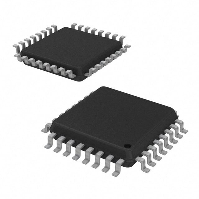
| 描述 | IC ADC 4.5 DGT LCD DVR 32LQFP模数转换器 - ADC 4.5 Digit ADC w/LCD Drivers |
| 产品分类 | |
| 品牌 | Maxim Integrated |
| 产品手册 | |
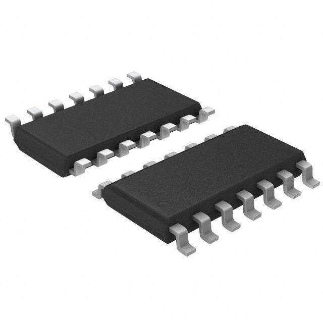
| 产品图片 |
|
| rohs | 符合RoHS无铅 / 符合限制有害物质指令(RoHS)规范要求 |
| 产品系列 | 数据转换器IC,模数转换器 - ADC,Maxim Integrated MAX1495CCJ+- |
| 数据手册 | |
| 产品型号 | MAX1495CCJ+ |
| 产品培训模块 | http://www.digikey.cn/PTM/IndividualPTM.page?site=cn&lang=zhs&ptm=25703http://www.digikey.cn/PTM/IndividualPTM.page?site=cn&lang=zhs&ptm=25705 |
| 产品目录页面 | |
| 产品种类 | 模数转换器 - ADC |
| 供应商器件封装 | 32-LQFP/32-TQFP (7x7) |
| 信噪比 | No |
| 分辨率 | 4.5 bit |
| 包装 | 托盘 |
| 商标 | Maxim Integrated |
| 安装类型 | 表面贴装 |
| 安装风格 | SMD/SMT |
| 封装 | Tube |
| 封装/外壳 | 32-LQFP |
| 封装/箱体 | LQFP-32 |
| 工作温度 | 0°C ~ 70°C |
| 工作电源电压 | 2.7 V to 5.25 V |
| 工厂包装数量 | 250 |
| 应用说明 | |
| 接口 | - |
| 接口类型 | Parallel |
| 数字或字符 | A/D,4.5 位数字 |
| 显示类型 | LCD |
| 最大功率耗散 | 1652.9 mW |
| 最大工作温度 | + 70 C |
| 最小工作温度 | 0 C |
| 标准包装 | 1 |
| 电压-电源 | 2.7 V ~ 5.25 V |
| 电压参考 | 2.048 V |
| 电流-电源 | 980µA |
| 系列 | MAX1495 |
| 结构 | Sigma-Delta |
| 转换器数量 | 1 |
| 转换速率 | 0.0025 kS/s |
| 输入类型 | Differential |
| 通道数量 | 1 Channel |
| 配置 | 7 段 + 2 个信号器 |
| 零件号别名 | MAX1495 |









PDF Datasheet 数据手册内容提取
19-3053; Rev 2; 5/04 EVAALVUAAILTAIOBNL EKIT 3.5- and 4.5-Digit, Single-Chip ADCs with LCD Drivers General Description Features M The MAX1491/MAX1493/MAX1495 low-power, 3.5- and ♦ High Resolution A 4.5-digit, analog-to-digital converters (ADCs) with inte- MAX1495: 4.5 Digits (±19,999 Count) X grated liquid crystal display (LCD) drivers operate from a MAX1493: 4.5 Digits (±19,999 Count) single 2.7V to 5.25V power supply. They include an inter- 1 MAX1491: 3.5 Digits (±1999 Count) nal reference, a high-accuracy on-chip oscillator, and a 4 triplexed LCD driver. An internal charge pump generates ♦ Sigma-Delta ADC Architecture 9 the negative supply needed to power the integrated input No Integrating Capacitors Required 1 buffer for single supply operation. The ADC is config- No Autozeroing Capacitors Required urable for either a ±2V or ±200mV input range and it out- >100dB of Simultaneous 50Hz and 60Hz Rejection /M puts its conversion results to an LCD. The MAX1491 is a ♦ Operate from a Single 2.7V or 5.25V Supply 3.5-digit (±1999 count) device, and the MAX1493/ A MAX1495 are 4.5-digit (±19,999 count) devices. ♦ Selectable Input Range of ±200mV or ±2V X The MAX1491/MAX1493/MAX1495 do not require exter- ♦ Selectable Voltage Reference: Internal 2.048V or 1 nal-precision integrating or auto-zero capacitors, crystal External 4 oscillators, charge pumps, or other circuitry required with dual slope ADCs (commonly used in panel meter ♦ Internal High-Accuracy Oscillator Needs No 9 circuits). These devices also feature on-chip buffers for External Components 3 the differential signal and reference inputs, allowing ♦ Automatic Offset Calibration /M direct interface with high-impedance signal sources. In addition, the MAX1491/MAX1493/MAX1495 use continu- ♦ Low Power: Maximum 980µA Operating Current A ous internal offset calibration, and offer >100dB rejec- tion of 50Hz and 60Hz line noise. The MAX1493/ ♦ Small 32-Pin 7mm ✕7mm TQFP Package (4.5 X MAX1495 perform enhanced offset calibration at power- Digits), 28-Pin SSOP Package (3.5 Digits), and 28- 1 up. The MAX1495 also performs enhanced calibration Pin DIP Package (3.5 Digits) 4 on demand. Other features include data hold and peak ♦ Triplexed LCD Driver 9 hold, and a user programmable low-battery monitor. ♦ Evaluation Kit Available (Order MAX1494EVKIT) 5 The MAX1493/MAX1495 come in a 32-pin 7mm ✕ 7mm TQFP package, and the MAX1491 comes in 28-pin SSOP and 28-pin DIP packages. All devices in this fam- Pin Configurations ily operate over the 0°C to +70°C commercial tempera- ture range. TOP VIEW GND DVDD INTREF VNEG DPON BP1 BP2 BP3 Applications 32 31 30 29 28 27 26 25 Digital Panel Meters AVDD 1 24 SEG13 Hand-Held Meters AIN+ 2 23 SEG12 Digital Voltmeters AIN- 3 22 SEG11 Digital Multimeters REF- 4 21 SEG10 MAX1493 REF+ 5 MAX1495 20 SEG9 Ordering Information LOWBATT 6 19 SEG8 RANGE 7 18 SEG7 TEMP PIN- RESOLUTION DPSET1 8 17 SEG6 PART RANGE PACKAGE (DIGITS) MAX1491CAI 0°C to +70°C 28 SSOP 3.5 9 10 11 12 13 14 15 16 MMAAXX11449913CCNCIJ 00°°CC ttoo ++7700°°CC 2382 DTQIPFP 34..55 DPSET2 PEAK HOLD SEG1 SEG2 SEG3 SEG4 SEG5 MAX1495CCJ 0°C to +70°C 32 TQFP 4.5 TQFP Pin Configurations continued at end of data sheet. ________________________________________________________________Maxim Integrated Products 1 For pricing, delivery, and ordering information,please contact Maxim/Dallas Direct!at 1-888-629-4642, or visit Maxim’s website at www.maxim-ic.com.
3.5- and 4.5-Digit, Single-Chip ADCs with LCD Drivers 5 ABSOLUTE MAXIMUM RATINGS 9 AVDDto GND............................................................-0.3V to +6V Continuous Power Dissipation (TA= +70°C) 4 DVDDto GND...........................................................-0.3V to +6V 32-Pin TQFP (derate 20.7mW/°C above +70°C).....1652.9mW 1 AIN+, AIN- to GND...............................VNEGto + (AVDD+ 0.3V) 28-Pin SSOP (derate 9.5mW/°C above +70°C)...........762mW REF+, REF- to GND..............................VNEGto + (AVDD+ 0.3V) 28-Pin DIP (derate 14.3mW/°C above +70°C)........1142.9mW X LOWBATT to GND...................................-0.3V to (AVDD+ 0.3V) Operating Temperature Range...............................0°C to +70°C INTREF, RANGE, DPSET1, DPSET2, PEAK, Junction Temperature......................................................+150°C A HOLD to GND......................................-0.3V to (DVDD+ 0.3V) Storage Temperature Range.............................-60°C to +150°C M DPON to GND..........................................-0.3V to (DVDD+ 0.3V) Lead Temperature (soldering, 10s).................................+300°C VNEGto GND...........................................-2.6V to (AVDD+ 0.3V) / Maximum Current into Any Pin ...........................................50mA 3 Stresses beyond those listed under “Absolute Maximum Ratings” may cause permanent damage to the device. These are stress ratings only, and functional 9 operation of the device at these or any other conditions beyond those indicated in the operational sections of the specifications is not implied. Exposure to 4 absolute maximum rating conditions for extended periods may affect device reliability. 1 ELECTRICAL CHARACTERISTICS X (AVDD= DVDD= +2.7V to +5.25V, GND = 0, VREF+- VREF-= 2.048V (external reference), CNEG= 0.1µF. All specifications are TMIN A to TMAX, unless otherwise noted. Typical values are at +25°C, unless otherwise noted.) M PARAMETER SYMBOL CONDITIONS MIN TYP MAX UNITS / DC ACCURACY 1 MAX1493/MAX1495 -19,999 +19,999 9 Noise-Free Resolution Count MAX1491 -1999 +1999 4 1 2.000V range ±1 Integral Nonlinearity (Note 1) INL Count X 200mV range ±1 A Range Change Accuracy (VAIN+ - VAIN- = 0.100V) on 200mV range / 10:1 Ratio (VAIN+ - VAIN- = 0.100V) on 2.0V range M VAIN+ - VAIN- = full scale, Rollover Error ±1.0 Count VAIN- - VAIN+ = full scale Output Noise 10 µVP-P Offset Error (Zero Input Reading) Offset VIN = 0 (Note 2) -0 +0 Reading Gain Error (Note 3) -0.5 +0.5 %FSR Offset Drift (Zero Reading Drift) VIN = 0 0.1 µV/°C Gain Drift ±1 ppm/°C INPUT CONVERSION RATE Conversion Rate 5 Hz ANALOG INPUTS (AIN+, AIN-) (bypass to GND with 0.1µF or greater capacitors) RANGE = GND -2.0 +2.0 Differential (Note 4) AIN Input Voltage Range RANGE = DVDD -0.2 +0.2 V Absolute GND referenced -2.2V +2.2V Normal Mode 50Hz and 60Hz 50Hz and 60Hz ±2% 100 dB Rejection (Simultaneously) Common-Mode 50Hz and 60Hz For 50Hz ±2% and 60Hz ±2%, CMR 150 dB Rejection (Simultaneously) RSOURCE < 10kΩ Common-Mode Rejection CMR At DC 100 dB Input Leakage Current TA = +25°C 10 nA Input Capacitance 10 pF Dynamic Input Current (Note 5) -20 +20 nA 2 _______________________________________________________________________________________
3.5- and 4.5-Digit, Single-Chip ADCs with LCD Drivers ELECTRICAL CHARACTERISTICS (continued) M (AVDD= DVDD= +2.7V to +5.25V, GND = 0, VREF+- VREF-= 2.048V (external reference), CNEG= 0.1µF. All specifications are TMIN A to TMAX, unless otherwise noted. Typical values are at +25°C, unless otherwise noted.) X PARAMETER SYMBOL CONDITIONS MIN TYP MAX UNITS 1 LOW-BATTERY VOLTAGE MONITOR (LOWBATT) 4 LOWBATT Trip Threshold 2.048 V 9 LOWBATT Leakage Current 10 pA 1 Hysteresis 20 mV / M INTERNAL REFERENCE (REF- = GND, INTREF = DVDD, bypass REF+ to GND with 4.7µF capacitors) REF Output Voltage VREF AVDD = 5V, TA = +25°C 2.007 2.048 2.089 V A REF Output Short-Circuit Current TA = +25°C 1 mA X REF Output Temperature TCVREF AVDD = 5V 40 ppm/°C 1 Coefficient 4 ISOURCE = 0µA to 300µA, 9 Load Regulation 6 mV/µA ISINK = 0µA to 30µA, TA = +25°C (Note 6) 3 Line Regulation 50 µV/V / M 0.1Hz to 10Hz 25 Noise Voltage µVp-p 10Hz to 10kHz 400 A EXTERNAL REFERENCE (INTREF = GND, bypass REF+ and REF- to GND with 0.1µF or greater capacitors) X Differential (VREF+ - VREF-) 2.048 1 REF Input Voltage V Absolute GND referenced -2.2 +2.2 4 Normal-Mode 50Hz and 60Hz 9 50Hz and 60Hz ±2% 100 dB Rejection (Simultaneously) 5 Common-Mode 50Hz and 60Hz For 50Hz ±2% and 60Hz ±2%, CMR 150 dB Rejection (Simultaneously) RSOURCE < 10kΩ Common-Mode Rejection CMR At DC 100 dB Input Leakage Current TA = +25°C 10 nA Input Capacitance 10 pF Dynamic Input Current (Note 5) -20 +20 nA CHARGE PUMP Output Voltage VNEG -2.6 -2.42 -2.3 V DIGITAL INPUTS (INTREF, RANGE, PEAK, HOLD, DPSET1, DPSET2, DPON) Input Current IIN VIN = 0 or DVDD -10 +10 µA 0.3 x Input Low Voltage VINL V DVDD 0.7 x Input High Voltage VINH V DVDD Input Hysteresis VHYS DVDD = 3.0V 200 mV _______________________________________________________________________________________ 3
3.5- and 4.5-Digit, Single-Chip ADCs with LCD Drivers 5 ELECTRICAL CHARACTERISTICS (continued) 9 (AVDD= DVDD= +2.7V to +5.25V, GND = 0, VREF+- VREF-= 2.048V (external reference), CNEG= 0.1µF. All specifications are TMIN 4 to TMAX, unless otherwise noted. Typical values are at +25°C, unless otherwise noted.) 1 PARAMETER SYMBOL CONDITIONS MIN TYP MAX UNITS X POWER SUPPLY A AVDD Voltage AVDD 2.70 5.25 V M DVDD Voltage DVDD 2.70 5.25 V Power-Supply Rejection AVDD PSRRA (Note 7) 80 dB / 3 Power-Supply Rejection DVDD PSRRD (Note 7) 100 dB 9 AVDD Current IAVDD (Note 8) 660 µA 4 DVDD = 5V 320 1 DVDD Current IDVDD µA DVDD = 3.3V 180 X LCD DRIVER A 1.92 x RMS Segment-On Voltage V M DVDD / 1 / 3 x 1 RMS Segment-Off Voltage V DVDD 9 Display Multiplex Rate 107 Hz 4 LCD Data-Update Rate 2.5 Hz 1 X Note 1: Integral nonlinearity is the derivation of the analog values at any code from its theoretical value after nulling the gain error and offset error. A Note 2: Offset calibrated. M Note 3: Offset nulled. Note 4: The input voltage range for the analog inputs is given with respect to the voltage on the negative input of the differential pair. Note 5: For the range of VAIN+or VAIN-= -2.2V to +2.2V and VREF+or VREF-= -2.2V to +2.2V. Note 6: External load must be constant during conversion for specified accuracy. Guaranteed specification of 2mV/mA is a result of production test limitations. Note 7: Measured at DC by changing the power-supply voltage from 2.7V to 5.25V and measuring its effect on the conversion error. PSRR at 50Hz and 60Hz exceeds 120dB with filter notches of 10, 20, 30, 40, 50, or 60Hz. Note 8: Analog power-supply currents are measured with all digital inputs at either GND or DVDD. Digital power-supply currents measured with all digital inputs at either GND or DVDD. 4 _______________________________________________________________________________________
3.5- and 4.5-Digit, Single-Chip ADCs with LCD Drivers Typical Operating Characteristics M (AVDD= DVDD= 5V, GND = 0, REF+ = 2.048V, REF- = GND, RANGE = DVDD, TA= +25°C.) A X MAX1493/MAX1495 (±200mV INPUT RANGE) MAX1493/MAX1495 (±2V INPUT RANGE) 1 INL vs. DISPLAY COUNT INL vs. DISPLAY COUNT NOISE DISTRIBUTION 4 01..50 MAX1491/3/5 toc01 01..50 MAX1491/3/5 toc02 S (%) 2205 MAX1491/3/5 toc03 91/M T UNTS) UNTS) OF UNI 15 A CO 0 CO 0 GE NL ( NL ( NTA 10 X I I E RC 1 -0.5 -0.5 PE 5 4 9 -1.0 -1.0 0 3 -20,000 -10,000 0 10,000 20,000 -20,000 -10,000 0 10,000 20,000 -0.2-0.1 0 0.10.20.30.40.50.60.70.8 / DISPLAY COUNT DISPLAY COUNT NOISE (COUNTS) M A X SUPPLY CURRENT MAX1493/MAX1495 MAX1493/MAX1495 1 vs. SUPPLY VOLTAGE GAIN ERROR vs. SUPPLY VOLTAGE GAIN ERROR vs. TEMPERATURE 4 µSUPPLY CURRENT (A) 234567000000000000 DANIGAITLAOLG SSUUPPPPLLYY MAX1491/3/5 toc04 GAIN ERROR (% FULL SCALE)---0000000.......000000004684262 MAX1491/3/5 toc05 GAIN ERROR (% FULL SCALE)--------00000000........00000000087654321 MAX1491/3/5 toc06 95 100 -0.08 -0.09 0 -0.10 -0.10 2.75 3.25 3.75 4.25 4.75 5.25 2.75 3.25 3.75 4.25 4.75 5.25 0 10 20 30 40 50 60 70 SUPPLY VOLTAGE (V) SUPPLY VOLTAGE (V) TEMPERATURE (°C) _______________________________________________________________________________________ 5
3.5- and 4.5-Digit, Single-Chip ADCs with LCD Drivers 5 Typical Operating Characteristics (continued) 9 (AVDD= DVDD= 5V, GND = 0, REF+ = 2.048V, REF- = GND, RANGE = DVDD, TA= +25°C.) 4 1 INTERNAL REFERENCE VOLTAGE INTERNAL REFERENCE VOLTAGE SUPPLY CURRENT X vs. TEMPERATURE vs. ANALOG SUPPLY VOLTAGE vs. TEMPERATURE X1493/MA REFERENCE VOLTAGE (V)22222222........000000004454555578291034 MAX1491/3/5 toc07 REFERENCE VOLTAGE (V)22222.....000004444567890 MAX1491/3/5 toc08 µSUPPLY CURRENT (A) 234567000000000000 ANALDOIGGI TSAULP SPULPYPLY MAX1491/3/5 toc09 2.046 A 2.045 100 2.045 M 2.044 2.044 0 0 10 20 30 40 50 60 70 2.75 3.25 3.75 4.25 4.75 5.25 0 10 20 30 40 50 60 70 1/ TEMPERATURE (°C) SUPPLY VOLTAGE (V) TEMPERATURE (°C) 9 4 1 X CHARGE-PUMP OUTPUT VOLTAGE OFFSET ERROR A vs. ANALOG SUPPLY VOLTAGE VNEG STARTUP SCOPE SHOT vs. COMMON-MODE VOLTAGE M --22..4420 MAX1491/3/5 toc10 2V/div VDD MAX1491/3/5 toc11 S) 000...112050 MAX1491/3/5 toc12 T V) UN V VOLTAGE (NEG--22..4464 1V/div VNEG FSET ERROR (CO-00..00055 F O-0.10 -2.48 -0.15 CNEG = 0.1µF -2.50 -0.20 2.75 3.25 3.75 4.25 4.75 5.25 20ms/div -2.0 -1.5 -1.0 -0.5 0 0.5 1.0 1.5 2.0 SUPPLY VOLTAGE (V) COMMON-MODE VOLTAGE (V) 6 _______________________________________________________________________________________
3.5- and 4.5-Digit, Single-Chip ADCs with LCD Drivers Pin Description M A PIN X NAME FUNCTION MAX1493 MAX1491 MAX1495 1 4 Internal Reference Logic Input. Connect to GND to select external reference mode. Connect 1 30 INTREF 9 to DVDD to select the internal reference mode. 1 Digital Power Input. Connect DVDD to a 2.7V to 5.25V power supply. Bypass DVDD to GND 2 31 DVDD / with a 0.1µF and a 4.7µF capacitor. M 3 32 GND Ground A 4 1 AVDD Analog Power Input. Connect AVDD to a 2.7V to 5.25V power supply. Bypass AVDD to GND X with a 0.1µF and a 4.7µF capacitor. 1 Positive Analog Input. Positive side of fully differential analog input. Bypass AIN+ to GND with 5 2 AIN+ 4 a 0.1µF or greater capacitor. 9 6 3 AIN- Negative Analog Input. Negative side of fully differential analog input. Bypass AIN- to GND 3 with a 0.1µF or greater capacitor. / M Negative Reference Input. For internal reference operation, connect REF- to GND. For 7 4 REF- external reference operation, bypass REF- to GND with a 0.1µF capacitor and set VREF- from A -2.2V to +2.2V, provided VREF+ > VREF-. X Positive Reference Input. For internal reference operation, connect a 4.7µF capacitor from 1 8 5 REF+ REF+ to GND. For external reference operation, bypass REF+ to GND with a 0.1µF capacitor 4 and set VREF+ from -2.2V to +2.2V, provided VREF+ > VREF-. 9 9 6 LOWBATT Low Batter y Inpu t. Wh en VL OWB ATT < 2.048V (t yp) , the LOW BATT symb o l on the LCD tur ns on. 5 Range Logic Input. RANGE controls the fully differential analog input range. Connect to GND 10 7 RANGE for the ±2V input range. Connect to DVDD for the ±200mV input range. Decimal Point Logic Input 1. Controls the decimal point of the LCD. See the Decimal Point 11 8 DPSET1 Control section. Decimal Point Logic Input 2. Controls the decimal point of the LCD. See the Decimal Point 12 9 DPSET2 Control section. Peak Logic Input. Connect to DVDD to display the highest ADC value on the LCD. Connect to 13 10 PEAK GND to disable the peak function. Hold Logic Input. Connect to DVDD to hold the current ADC value on the LCD. Connect to GND to update the LCD at a rate of 2.5Hz and disable the hold function. For the MAX1495, 14 11 HOLD placing the device into hold mode initiates an enhanced offset calibration. Assert HOLD high for a minimum of 2s to ensure the completion of enhanced offset calibration. 15 12 SEG1 LCD Segment 1 Driver 16 13 SEG2 LCD Segment 2 Driver 17 14 SEG3 LCD Segment 3 Driver 18 15 SEG4 LCD Segment 4 Driver 19 16 SEG5 LCD Segment 5 Driver 20 17 SEG6 LCD Segment 6 Driver _______________________________________________________________________________________ 7
3.5- and 4.5-Digit, Single-Chip ADCs with LCD Drivers 5 Pin Description (continued) 9 PIN 4 1 MAX1493 NAME FUNCTION MAX1491 X MAX1495 21 18 SEG7 LCD Segment 7 Driver A 22 19 SEG8 LCD Segment 8 Driver M 23 20 SEG9 LCD Segment 9 Driver / 3 24 21 SEG10 LCD Segment 10 Driver 9 25 25 BP3 LCD Backplane 3 Driver 4 26 26 BP2 LCD Backplane 2 Driver 1 27 27 BP1 LCD Backplane 1 Driver X 28 29 VNEG -2.5V Charge-Pump Voltage Output. Connect a 0.1µF capacitor from VNEG to GND. A — 22 SEG11 LCD Segment 11 Driver M — 23 SEG12 LCD Segment 12 Driver — 24 SEG13 LCD Segment 13 Driver / 1 Decimal Point Enable Input. Controls the decimal point of the LCD. See the Decimal Point — 28 DPON 9 Control section. Connect to DVDD to enable the decimal point. 4 1 X DPON HOLD DPSET1 DPSET2 RANGE PEAK INTREF AVDD DVDD A M MAX1493 MAX1495 CONTROL +2.5V SEG1 AIN+ BINARY-TO-BCD CONVERTERS ADC SEG13 AND BP1 AIN- LCD DRIVERS BP2 BP3 INPUT BUFFERS REF+ REF- OSCILLATOR/ CLOCK TO CONTROL -2.5V +2.5V -2.5V 2.048V CHARGE BANDGAP A = 1.22 PUMP REFERENCE GND VNEG LOWBATT Figure 1. MAX1493/MAX1495 Functional Diagram 8 _______________________________________________________________________________________
3.5- and 4.5-Digit, Single-Chip ADCs with LCD Drivers Detailed Description Digital Filtering M The MAX1491/MAX1493/MAX1495 contain an on-chip The MAX1491/MAX1493/MAX1495 low-power, highly A digital lowpass filter that processes the data stream integrated ADCs with LCD drivers convert a ±2V differ- from the modulator using a SINC4 (sinx/x)4 response. X ential input voltage (one count is equal to 100µV for the The SINC4 filter has a settling time of four output data MAX1493/MAX1495 and 1mV for the MAX1491) with a 1 periods (4 x 200ms). sigma-delta ADC and output the result to an LCD. An 4 additional ±200mV input range (one count is equal to The MAX1491/MAX1493/MAX1495 have 25% overrange 9 10µV for the MAX1493/MAX1495 and 100µV for the capability built into the modulator and digital filter: 1 MAX1491) is available to measure small signals with 4 increased resolution. ⎡⎢ sin⎛⎜Nπ f ⎞⎟⎤⎥ /M These devices operate from a single 2.7V to 5.25V power H(f)=⎢⎢1 ⎝ fm⎠⎥⎥ A s(MupApXl1y4 9a3n/dM AofXf1e4r 935.)5 -cdoingvite r(sMioAnX r1e4s9u1lt)s .o Ar n4 .in5t-edringaitl ⎣⎢⎢N sin⎛⎝⎜πfmf ⎞⎠⎟ ⎦⎥⎥ X 2.048V reference, internal charge pump and a high-accu- 1 racy on-chip oscillator eliminate external components. ( ) 4 4 These devices also feature on-chip buffers for the dif- ⎡⎢1 1-z-N ⎤⎥ 9 ferential input signal and external reference inputs, H(z)=⎢ ( )⎥ 3 allowing direct interface with high-impedance signal ⎢N 1-z-1 ⎥ sources. In addition, they use continuous internal offset ⎣ ⎦ /M calibration, and offer >100dB of 50Hz and 60Hz line noise rejection. Other features include data hold and Filter Characteristics A peak hold, and a low-battery monitor. The MAX1495 Figure 2 shows the filter frequency response. The SINC4 X also performs enhanced offset calibration on demand. characteristic -3dB cutoff frequency is 0.228 times the first notch frequency (5Hz). The oversampling ratio 1 Analog Input Protection (OSR) for the MAX1491 is 128 and the OSR for the 4 Internal protection diodes limit the analog input range MAX1493/MAX1495 is 1024. 9 from VNEG to (AVDD + 0.3V). If the analog input The output data rate for the digital filter corresponds 5 exceeds this range, limit the input current to 10mA. with the positioning of the first notch of the filter’s fre- Internal Analog Input/ quency response. The notches of the SINC4 filter are Reference Buffers repeated at multiples of the first notch frequency. The The MAX1491/MAX1493/MAX1495 analog input/refer- SINC4 filter provides an attenuation of better than ence buffers allow the use of high-impedance signal 100dB at these notches. For example, 50Hz is equal to sources. The input buffers’ common-mode input range 10 times the first notch frequency and 60Hz is equal to allows the analog inputs and reference to range from 12 times the first notch frequency. -2.2V to +2.2V. Modulator 0 The MAX1491/MAX1493/MAX1495 perform analog-to- digital conversions using a single-bit, 3rd-order, sigma- -40 delta modulator. The sigma-delta modulation converts the input signal into a digital pulse train whose average duty cycle represents the digitized signal information. dB) -80 The modulator quantizes the input signal at a much AIN ( higher sample rate than the bandwidth of the input. G-120 The MAX1491/MAX1493/MAX1495 modulator provides 3rd-order frequency shaping of the quantization noise -160 resulting from the single-bit quantizer. The modulator is fully differential for maximum signal-to-noise ratio and -200 minimum susceptibility to power-supply noise. A single- 0 10 20 30 40 50 60 FREQUENCY (Hz) bit data stream is then presented to the digital filter for processing, to remove the frequency-shaped quantiza- Figure 2. Frequency Response of the SINC4Filter (Notch at 60Hz) tion noise. _______________________________________________________________________________________ 9
3.5- and 4.5-Digit, Single-Chip ADCs with LCD Drivers 5 Internal Clock The MAX1491/MAX1493/MAX1495 contain an internal 9 X Y Z oscillator. Using the internal oscillator saves board 4 space by removing the need for an external clock 1 source. The oscillator is optimized to give 50Hz and X 60Hz power supply and common-mode rejection. A Charge Pump a a M The MAX1491/MAX1493/MAX1495 contain an internal f b BP1 f b charge pump to provide the negative supply voltage for / 3 the internal analog input/reference buffers. The bipolar g g input range of the analog input/reference buffers allows 9 4 the devices to accept negative inputs with high source e c BP2 e c impedances. For the charge pump to operate correctly, 1 connect a 0.1µF capacitor from VNEGto GND. d d X LCD Driver A DP ANNUNCIATOR The MAX1491/MAX1493/MAX1495 contain the neces- BP3 M sary backplane and segment driver outputs to drive DP ANNUNCIATOR 3.5-digit (MAX1491) and 4.5-digit (MAX1493/MAX1495) / 1 LCDs. The LCD update rate is 2.5Hz. Figures 4–7 show 9 the connection schemes for a standard LCD. The Figure 3. Connection Diagrams for Typical Seven-Segment Displays MAX1491/MAX1493/MAX1495 automatically display the 4 results of the ADC. 1 with BP2 to form the g segment, and with BP3 to form X Triplexing the d segment. Eight different ON/OFF combinations of An internal resistor string of three equal-value resistors the a, g, and d segments and their corresponding A (52kΩ, 1% matching) is used to generate the display waveforms of the y segment line are illustrated in M drive voltages. One end of the string is connected to Figures 9 and 10. The schematic diagram in Figure 8 DVDDand the other end is connected to GND. Note that shows that each intersection acts as a capacitance VLCD (VLCD = DVDD - GND) should be three times the from segment line to common line. Figure 11 illustrates threshold voltage for the liquid-crystal material used. the voltage across the g segment. The connection diagram for a typical 7-segment display The RMS voltage across the segment determines the font with two annunciators is illustrated in Figure 3 and degree of polarization for the liquid-crystal material and Figure 8. The MAX1491/MAX1493/MAX1495 numeric thus the contrast of the segment. The RMS OFF voltage display drivers (4.5 digits, 3.5 digits) use this configura- is always VLCD / 3, whereas the RMS ON voltage is tion to drive a triplexed LCD with three backplanes and always 1.92VLCD/ 3. This is illustrated in Figure 11. The 13 segment driver lines (10 for 3.5 digits). Figures 4 and ratio of RMS ON to OFF voltage is fixed at 1.92 for a 5 show the assignment of the 4.5-digit display segments triplexed LCD. and Figures 6 and 7 show the assignment of the 3.5- Figure 12 illustrates contrast vs. applied RMS voltage digit display segments. with a VLCD of 3.1V. The RMS ON voltage is 2.1V and The voltage waveforms of the backplane lines and y the RMS OFF voltage is 1.1V. The OFF segment has a segment line (Figure 3) have been chosen as an exam- contrast of less than 5%, while the ON segments have ple. This line intersects with BP1 to form the a segment, greater than 85% contrast. Table 1. List of LCD Manufacturers MANUFACTURER WEBSITE PART NUMBER DESCRIPTION 04-0924-00 3.5 digit, 5V 04-0924-01 3.5 digit, 3V DCI, Inc. www.dciincorporated.com 04-0925-00 4.5 digit, 5V 04-0925-01 4.5 digit, 3V The following site has links to other custom LCD manufacturers: www.earthlcd.com/mfr.htm 10 ______________________________________________________________________________________
3.5- and 4.5-Digit, Single-Chip ADCs with LCD Drivers M A X HOLD PEAK LOW BATT 1 4 9 BP1 1 / M A BP2 X 1 4 BP3 9 3 / Figure 4. Backplane Connection for the MAX1493/MAX1495 (4.5 Digits) M A X SEG13: PEAK, HOLD, N.C. 1 4 9 HOLD PEAK LOW BATT SEG2: A1, G1, D1 5 ANNUNCIATOR SEG12: F4, E4, DP4 SEG1: B1, C1, ANNUNCIATOR SEG11: A4, G4, D4 SEG3: F1, E1, DP1 SEG10: B4, C4, BC5 SEG4: B2, C2, LOWBATT SEG9: F3, E3, DP3 SEG5: A2, G2, D2 SEG8: A3, G3, D3 SEG6: F2, E2, DP2 SEG7: B3, C3, MINUS Figure 5. Segment Connection for the MAX1493/MAX1495 (4.5 Digits) ______________________________________________________________________________________ 11
3.5- and 4.5-Digit, Single-Chip ADCs with LCD Drivers 5 9 4 HOLD PEAK LOW BATT 1 X A BP1 M / 3 BP2 9 4 1 BP3 X Figure 6. Backplane Connection for the MAX1491 (3.5 Digits) A M SEG10: PEAK, HOLD, BC4 / 1 HOLD PEAK LOW BATT SEG2: A1, G1, D1 ANNUNCIATOR 9 4 1 X A M SEG1: B1, C1, ANNUNCIATOR SEG3: F1, E1, DP1 SEG4: B2, C2, LOWBATT SEG9: F3, E3, DP3 SEG5: A2, G2, D2 SEG8: A3, G3, D3 SEG6: F2, E2, DP2 SEG7: B3, C3, MINUS Figure 7. Segment Connection for the MAX1491 (3.5 Digits) X Y Z f a b BP1 e g c BP2 DP d DP BP3 Figure 8. Schematic of Display Digit 12 ______________________________________________________________________________________
3.5- and 4.5-Digit, Single-Chip ADCs with LCD Drivers M φ1 φ2 φ3 φ1' φ2' φ3' A X V+ 1 VH BP1 VLCD 4 VL 9 V- 1 V+ / M VH BP2 A VL X V- 1 V+ 4 VH 9 BP3 3 VL / V- M V+ A ALL VH X OFF VL 1 4 V- 9 V+ 5 a ON VH g, d OFF VL V- V+ g ON VH a, d OFF VL V- V+ d ON VH a, g OFF VL V- FREQUENCY = 107Hz φ1, φ2, φ3 - - BP HIGH WITH RESPECT TO SEGMENT (BP+ TIME) V+ = DVDD, VH = 2/3 DVDD φ1', φ2', φ3' - - BP LOW WITH RESPECT TO SEGMENT (BP- TIME) VL = 1/3 VLCD, V- = GND BP1 ACTIVE DURING φ1 AND φ1' VLCD = DVDD - GND BP2 ACTIVE DURING φ2 AND φ2' BP3 ACTIVE DURING φ3 AND φ3' Figure 9. LCD Voltage Waveform—Combinations 1–4 (BP1/2/3, SEGa/d/g) ______________________________________________________________________________________ 13
3.5- and 4.5-Digit, Single-Chip ADCs with LCD Drivers 5 9 φ1 φ2 φ3 φ1' φ2' φ3' 4 V+ 1 X VH BP1 VLCD A VL M V- / V+ 3 VH 9 BP2 4 VL 1 V- X V+ A VH BP3 M VL / V- 1 V+ 9 4 ALL VH 1 OFF VL X V- A V+ M a, d ON VH g OFF VL V- V+ a, g ON VH d OFF VL V- V+ g, d ON VH a OFF VL V- FREQUENCY = 107Hz φ1, φ2, φ3 - - BP HIGH WITH RESPECT TO SEGMENT (BP+ TIME) V+ = DVDD, VH = 2/3 DVDD φ1', φ2', φ3' - - BP LOW WITH RESPECT TO SEGMENT (BP- TIME) VL = 1/3 VLCD, V- = GND BP1 ACTIVE DURING φ1 AND φ1' VLCD = DVDD - GND BP2 ACTIVE DURING φ2 AND φ2' BP3 ACTIVE DURING φ3 AND φ3' Figure 10. LCD Voltage Waveform—Combinations 5–8 (BP1/2/3, SEGa/d/g) 14 ______________________________________________________________________________________
3.5- and 4.5-Digit, Single-Chip ADCs with LCD Drivers M φ1 φ2 φ3 φ1' φ2' φ3' A VLCD X 1 4 ALL 0 VRMS = VLCD / 3 (OFF) 9 OFF 1 / M -VLCD A X VLCD 1 4 9 g, da O OFNF 0 VRMS = VLCD / 3 (OFF) 3 / M A -VLCD X VLCD 1 4 9 a, g ON 5 d OFF 0 VRMS = 1.92VLCD / 3 (ON) -VLCD VLCD ALL ON 0 VRMS = 1.92VLCD / 3 (ON) -VLCD VG = VY - VBP2 (DIFFERENCE BETWEEN SEGMENT LINE Y AND BP2 VOLTAGE) VOLTAGE CONTRAST RATIO = VRMS ON / VRMSOFF = 1.922 φ1, φ2, φ3 - - BP HIGH WITH RESPECT TO SEGMENT (BP+ TIME) φ1', φ2', φ3' - - BP LOW WITH RESPECT TO SEGMENT (BP- TIME) BP1 ACTIVE DURING φ1 AND φ1' BP2 ACTIVE DURING φ2 AND φ2' BP3 ACTIVE DURING φ3 AND φ3' Figure 11. Voltage Waveforms on the g Segment ______________________________________________________________________________________ 15
3.5- and 4.5-Digit, Single-Chip ADCs with LCD Drivers 5 9 4 100 1 X 90 Ø = -10°C A 80 M 70 Ø = +10°C 3/ %) 60 Ø = -30°C Ø = 0°C 9 ST ( 50 A R 4 T ON 40 1 C X 30 VOFF = A 20 1.1VRMS VON = 2.1VRMS M 10 TA = +25°C / 0 1 0 1 2 3 4 5 9 APPLIED VOLTAGE (VRMS) 4 1 X A M Ø+ Ø- Figure 12. Contrast vs. Applied RMS Voltage 16 ______________________________________________________________________________________
3.5- and 4.5-Digit, Single-Chip ADCs with LCD Drivers If ghosting is present on the LCD, the RMS OFF voltage Connect INTREF to GND to use the external reference. M is too high. Choose an LCD with a higher RMS OFF The external reference inputs, REF+ and REF-, are fully voltage or decrease DVDD. differential. For a valid external reference input, VREF+ A must be greater than VREF-. Bypass REF+ and REF- X Decimal Point Control with a 0.1µF or greater capacitor to GND in external ref- The MAX1491/MAX1493/MAX1495 allow for full deci- 1 erence mode. mal-point control and feature leading-zero suppression. 4 Figure 13 shows the MAX1493/MAX1495 operating with Use DPON, DPSET1, and DPSET2 to set the value of 9 an external differential reference. In this mode, REF- is the decimal point. Tables 2 and 3 show the truth tables connected to the top of the strain gauge and REF+ is 1 of the DPON, DPSET1, and DPSET2 that determine connected to the midpoint of the resistor-divider on the / which decimal point is used. M supply. Reference Applications Information A The MAX1491/MAX1493/MAX1495 reference sets the X full-scale range of the ADC transfer function. With a Power-On nominal 2.048V reference, the ADC full-scale range is 1 At power-on, the digital filter and modulator circuits ±2V with RANGE equal to GND. With RANGE equal to reset. The MAX1493/MAX1495 allow 6s for the refer- 4 DVDD, the full-scale range is ±200mV. A decreased ref- ence to stabilize before performing enhanced offset 9 erence voltage decreases full-scale range (see the calibration. During these 6s, the MAX1493/MAX1495 3 Transfer Functionssection). display 1.2V to 1.5V when a stable reference is detect- / The MAX1491/MAX1493/MAX1495 accept either an ed. If a valid reference is not found, the MAX1493/ M external reference or an internal reference. The INTREF MAX1495 time out after 6s and begin enhanced offset A input selects the reference mode. calibration. Enhanced offset calibration typically lasts 2s. The MAX1493/MAX1495 begin converting after X For internal reference operation, connect INTREF to DVDD, connect REF- to GND, and bypass REF+ to enhanced offset calibration. 1 GND with a 4.7µF capacitor. The internal reference pro- Offset Calibration 4 vides a nominal 2.048V source between REF+ and The MAX1491/MAX1493/MAX1495 offer on-chip offset 9 GND. The internal reference temperature coefficient is calibration. The MAX1491/MAX1493/MAX1495 calibrate 5 typically 40ppm/°C. offset during every conversion cycle. The MAX1495 Table 2. Decimal-Point Control Table (MAX1493/MAX1495) DPON DPSET1 DPSET2 DISPLAY OUTPUT ZERO INPUT READING 0 0 0 1 8 8 8 8 0 0 0 1 1 8 8 8 8 0 0 1 0 1 8 8 8 8 0 0 1 1 1 8 8 8 8 0 1 0 0 1 8 8 8.8 0.0 1 0 1 1 8 8.8 8 0.00 1 1 0 1 8.8 8 8 0.000 1 1 1 1.8 8 8 8 0.0000 Table 3. Decimal-Point Control Table (MAX1491) DPSET1 DPSET2 DISPLAY OUTPUT ZERO INPUT READING 0 0 1 8 8.8 0.0 0 1 1 8.8 8 0.00 1 0 1.8 8 8 0.000 1 1 1 8 8 8 000 ______________________________________________________________________________________ 17
3.5- and 4.5-Digit, Single-Chip ADCs with LCD Drivers 5 offers enhanced offset calibration on demand. Connect 9 HOLD to DVDD for 2s to perform enhanced offset cali- ANALOG SUPPLY bration. 4 FERRITE 1 Peak BEAD 0.1µF 4.7µF X The MAX1491/MAX1493/MAX1495 feature peak detec- 0.1µF 4.7µF tion circuitry. When activated (PEAK connected to DVDD), A the devices display only the highest voltage measured to AVDD DVDD M the LCD. First, the current ADC result is displayed. Then the new ADC conversion result is compared to this value. REF+ 3/ If the new value is larger than the previous peak value, 0.1µF the new value is displayed. If the new value is less than RREF MAX1491 9 the previous peak value, the display remains unchanged. MAX1493 4 Connect PEAK to GND to clear the peak value and dis- REF- MAX1495 VNEG 1 0.1µF 0.1µF able the peak function. The peak function is only valid for X the -19,487 to +19,999 range for the MAX1493/ ACTIVE R GAUGE A MAX1495 and -1217 to +1999 for the MAX1491. AIN+ M Hold 0.1µF AIN- The MAX1491/MAX1493/MAX1495 feature data HOLD DUMMY 0.1µF / GAUGE 1 circuitry. When activated (HOLD connected to DVDD), R the devices hold the current reading on the LCD. 9 GND INTREF 4 Low Battery 1 The MAX1491/MAX1493/MAX1495 feature a low-battery X detection input. When the voltage at LOWBATT drops below 2.048V (typ), the LOWBATT segment of the LCD A turns on. M Figure 13. Strain-Gauge Application with the MAX1491/MAX1493/ Strain Gauge Measurement MAX1495 Connect the differential inputs of the MAX1491/ MAX1493/MAX1495 to the bridge network of the strain gauge. In Figure 13, the analog supply voltage powers the bridge network and the MAX1491/MAX1493/ MAX1495 along with its reference voltage. The MAX1491/MAX1493/MAX1495 handle an analog input voltage range of ±200mV or ±2V full scale. The ana- log/reference inputs of the part allow the analog input range to have an absolute value anywhere between R = 100Ω for ±2V RANGE -2.2V and +2.2V. 10Ω for ±200mV RANGE 4–20mA Measurement To measure 4–20mA signals, connect a shunt resistor across AIN+ and AIN- to create the ±2V or ±200mV AIN+ input voltage (see Figure 14). 0.1µF 4–20mA R MAX1491 MAX1493 MAX1495 AIN- Table 4. LCD Priority Table 0.1µF HOLD PEAK DISPLAYS DVDD X Current value ±1.8.8.8.8 GND DVDD Peak value GND GND Latest ADC result Figure 14. 4–20mA Measurement 18 ______________________________________________________________________________________
3.5- and 4.5-Digit, Single-Chip ADCs with LCD Drivers Transfer Functions The transfer function for the MAX1493/MAX1495 with M Figures 15–18 show the MAX1491/MAX1493s’ transfer AIN+ - AIN- ≥0 and RANGE = DVDDis: functions. The transfer function for the MAX1493/ A MAX1495 with AIN+ - AIN- ≥0 and RANGE = GND is: Counts=1.024 × ⎛⎜ VAIN+-VAIN- ⎞⎟ × 20,000×10 X Counts=1.024 ×⎛⎜ VAIN+-VAIN- ⎞⎟ × 20,000 ⎝VREF+-VREF-⎠ 14 ⎝VREF+-VREF-⎠ The transfer function for the MAX1493 with AIN+ - AIN- 9 < 0 and RANGE = DVDDis: The transfer function for the MAX1493 with AIN+ - AIN- 1 < 0 and RANGE = GND is: Counts=1.024 ×⎛⎜ VAIN+-VAIN- × 20,000⎞⎟ ×10 +1 /M Counts=1.024 × ⎛⎜ VAIN+-VAIN- × 20,000⎞⎟ +1 ⎝VREF+-VREF- ⎠ A ⎝VREF+-VREF- ⎠ The transfer function for the MAX1491 with AIN+ - AIN- X ≥0 and RANGE = DVDDis: 1 The transfer function for the MAX1491 with AIN+ - AIN- ≥0 and RANGE = GND is: Counts=1.024 × ⎛⎜ VAIN+-VAIN- ⎞⎟ × 2000 ×10 49 Counts=1.024 × ⎛⎜ VAIN+-VAIN- ⎞⎟ × 2000 ⎝VREF+-VREF-⎠ 3 ⎝VREF+-VREF-⎠ The transfer function for the MAX1491 with AIN+ - AIN- /M < 0 and RANGE = DVDDis: The transfer function for the MAX1491 with AIN+ - AIN- A < 0 and RANGE = GND is: Counts=1.024 × ⎛⎜ VAIN+-VAIN- × 2000⎞⎟ × 10 + 1 X Counts=1.024 × ⎛⎜ VAIN+-VAIN- × 2000⎞⎟ +1 ⎝VREF+-VREF- ⎠ 1 ⎝VREF+-VREF- ⎠ 4 9 5 LCD LCD 1 - - - - 1 - - - - 19,999 19,999 2 2 1 1 0 0 - 0 - 0 - 1 - 1 - 2 - 2 -19,999 -19,999 - 1 - - - - - 1 - - - - -2V -100µV 0100µV +2V -200mV -10µV 0 10µV +200mV ANALOG INPUT VOLTAGE ANALOG INPUT VOLTAGE Figure 15. MAX1493/MAX1495 Transfer Function ±2V Range Figure 16. MAX1493/MAX1495 Transfer Function ±200mV Range ______________________________________________________________________________________ 19
3.5- and 4.5-Digit, Single-Chip ADCs with LCD Drivers 5 9 LCD LCD 4 1 - - - 1 - - - 1 1999 1999 X A 2 2 1 1 M 0 0 / - 0 - 0 3 - 1 - 1 9 - 2 - 2 4 1 -1999 -1999 X - 1 - - - - 1 - - - A -200mV -100µV 0100µV +200mV -2V -1mV 0 1mV +2V M ANALOG INPUT VOLTAGE ANALOG INPUT VOLTAGE / Figure 17. MAX1491 Transfer Function ±200mV Range Figure 18. MAX1491 Transfer Function ±2V Range 1 9 Supplies, Layout, and Bypassing Definitions 4 Power up AVDD and DVDD before applying an analog 1 input and external reference voltage to the device. If INL X this is not possible, limit the current into these inputs to Integral nonlinearity (INL) is the deviation of the values 50mA. Isolate the digital supply from the analog supply on an actual transfer function from a straight line. This A with a low-value resistor (10Ω) or ferrite bead when the straight line is either a best-straight-line fit or a line M analog and digital supplies come from the same drawn between the end points of the transfer function, source. For best performance, ground the MAX1491/ once offset and gain errors have been nullified. INL for MAX1493/MAX1495 to the analog ground plane of the the MAX1491/MAX1493/MAX1495 is measured using circuit board. the end-point method. Avoid running digital lines under the device, because DNL these may couple noise onto the die. Run the analog Differential nonlinearity (DNL) is the difference between ground plane under the MAX1491/MAX1493/MAX1495 an actual step width and the ideal value of one count. A to minimize coupling of digital noise. Make the power- DNL error specification of less than one count guarantees supply lines to the MAX1491/MAX1493/MAX1495 as no missing counts and a monotonic transfer function. wide as possible to provide low-impedance paths and reduce the effects of glitches on the power-supply line. Rollover Error Rollover error is defined as the absolute value differ- Shield fast-switching signals, such as clocks, with digital ence between a near-positive full-scale reading and ground to avoid radiating noise to other sections of the near-negative full-scale reading. Rollover error is tested board. Avoid running clock signals near the analog by applying a full-scale positive voltage, swapping inputs. Avoid crossover of digital and analog signals. AIN+ and AIN-, and then adding the results. Running traces that are on opposite sides of the board at right angles to each other reduces feedthrough effects. Zero Input Reading Good decoupling is important when using high-resolu- Ideally, with AIN+ connected to AIN-, the MAX1491/ tion ADCs. Decouple the supplies with 4.7µF and 0.1µF MAX1493/MAX1495 display a zero. Zero input reading ceramic capacitors to GND. Place these components is the measured deviation from the ideal zero and the as close to the device as possible to achieve the actual measured point. best decoupling. Refer to the MAX1494 evaluation kit manual for the rec- ommended layout. The evaluation board package includes a fully assembled and tested evaluation board. 20 ______________________________________________________________________________________
3.5- and 4.5-Digit, Single-Chip ADCs with LCD Drivers Gain Error MAX1493/MAX1495 sigma-delta converter uses its inter- M Gain error is the amount of deviation between the mea- nal digital filter to provide normal mode rejection to both sured full-scale transition point and the ideal full-scale 50Hz and 60Hz power-line frequencies simultaneously. A transition point. X Power-Supply Rejection Ratio Common-Mode Rejection Power-supply rejection ratio (PSRR) is the ratio of the 1 Common-mode rejection is the ability of a device to input supply change (in volts) to the change in the con- 4 reject a signal that is common to both input terminals. verter output (in volts). It is measured typically 9 The common-mode signal can be either an AC or a DC in decibels. 1 signal or a combination of the two. CMR is often Enhanced Offset Calibration / expressed in decibels. M Enhanced offset calibration is a more accurate calibra- Normal-Mode 50Hz and 60Hz Rejection tion method that is needed in the case of the ±200mV A (Simultaneously) range and 4.5-digit resolution. The MAX1493/MAX1495 X Normal mode rejection is a measure of how much output perform the enhanced offset calibration upon power-up. changes when 50Hz and 60Hz signals are injected into The MAX1495 also performs enhanced offset calibration 1 just one of the differential inputs. The MAX1491/ on demand with the HOLD input. 4 9 3 Typical Operating Circuit / M A HOLD PEAK LOW BATTERY X 1 4 9 5 SEG1–SEG13 BACKPLANE AIN+ (SEG1–SEG10) CONNECTIONS DVDD VIN AIN- INTREF 0.1µF 0.1µF PEAK MAX1493 HOLD DVDD MAX1495 DPON 4.7µF 0.1µF (MAX1491) DPSET1 DPSET2 AVDD 4.7µF LOWBATT VNEG GND REF- REF+ RANGE LISO RHI 0.1µF 4.7µF 2.7V TO 10µF 5.25V RLOW ______________________________________________________________________________________ 21
3.5- and 4.5-Digit, Single-Chip ADCs with LCD Drivers 5 Pin Configurations (continued) Chip Information 9 TRANSISTOR COUNT: 79,435 4 TOP VIEW PROCESS: BiCMOS 1 INTREF 1 28 VNEG X DVDD 2 27 BP1 A GND 3 26 BP2 M AVDD 4 25 BP3 / AIN+ 5 24 SEG10 3 MAX1491 AIN- 6 23 SEG9 9 REF- 7 22 SEG8 4 REF+ 8 21 SEG7 1 X LOWBATT 9 20 SEG6 A RANGE 10 19 SEG5 DPSET1 11 18 SEG4 M DPSET2 12 17 SEG3 / 1 PEAK 13 16 SEG2 9 HOLD 14 15 SEG1 4 SSOP OR DIP 1 X A M 22 ______________________________________________________________________________________
3.5- and 4.5-Digit, Single-Chip ADCs with LCD Drivers Package Information M (The package drawing(s) in this data sheet may not reflect the most current specifications. For the latest package outline information A go to www.maxim-ic.com/packages.) X PS 1 E FP. 4 Q T 8L, 9 4 2L/ 1 3 / M A X 1 4 9 3 / M A X 1 4 9 5 ______________________________________________________________________________________ 23
3.5- and 4.5-Digit, Single-Chip ADCs with LCD Drivers 5 Package Information (continued) 9 (The package drawing(s) in this data sheet may not reflect the most current specifications. For the latest package outline information 4 go to www.maxim-ic.com/packages.) 1 X 2 1 OP.EPS A SS M INCHES MILLIMETERS DIM MIN MAX MIN MAX INCHES MILLIMETERS / 3 A 0.068 0.078 1.73 1.99 MIN MAX MIN MAX N A1 0.002 0.008 0.05 0.21 D 0.239 0.249 6.07 6.33 14L 9 B 0.010 0.015 0.25 0.38 D 0.239 0.249 6.07 6.33 16L 4 C 0.004 0.008 0.09 0.20 D 0.278 0.289 7.07 7.33 20L 1 E H D SEE VARIATIONS D 0.317 0.328 8.07 8.33 24L X E 0.205 0.212 5.20 5.38 D 0.397 0.407 10.07 10.33 28L A e 0.0256 BSC 0.65 BSC H 0.301 0.311 7.65 7.90 M L 0.025 0.037 0.63 0.95 0∞ 8∞ 0∞ 8∞ / 1 9 N 4 1 X A A M C B e A1 L D NOTES: 1. D&E DO NOT INCLUDE MOLD FLASH. 2. MOLD FLASH OR PROTRUSIONS NOT TO EXCEED .15 MM (.006"). 3. CONTROLLING DIMENSION: MILLIMETERS. PROPRIETARY INFORMATION TITLE: 4. MEETS JEDEC MO150. PACKAGE OUTLINE, SSOP, 5.3 MM 5. LEADS TO BE COPLANAR WITHIN 0.10 MM. APPROVAL DOCUMENT CONTROL NO. REV. 1 21-0056 C 1 24 ______________________________________________________________________________________
3.5- and 4.5-Digit, Single-Chip ADCs with LCD Drivers Package Information (continued) M (The package drawing(s) in this data sheet may not reflect the most current specifications. For the latest package outline information A go to www.maxim-ic.com/packages.) X 1 S EP 4 N. P 9 DI P 1 / M A X 1 4 9 3 / M A X 1 4 9 5 Maxim cannot assume responsibility for use of any circuitry other than circuitry entirely embodied in a Maxim product. No circuit patent licenses are implied. Maxim reserves the right to change the circuitry and specifications without notice at any time. Maxim Integrated Products, 120 San Gabriel Drive, Sunnyvale, CA 94086 408-737-7600 ____________________25 © 2004 Maxim Integrated Products Printed USA is a registered trademark of Maxim Integrated Products.
Mouser Electronics Authorized Distributor Click to View Pricing, Inventory, Delivery & Lifecycle Information: M axim Integrated: MAX1491CAI+ MAX1491CAI+T MAX1493CCJ+T MAX1495CCJ+T MAX1491CNI+ MAX1493CCJ+ MAX1495CCJ+ MAX1495EEVKIT+