ICGOO在线商城 > MAX15007AATT+T

 Datasheet下载
- 型号: MAX15007AATT+T
- 制造商: Maxim
- 库位|库存: xxxx|xxxx
- 要求:
| 数量阶梯 | 香港交货 | 国内含税 |
| +xxxx | $xxxx | ¥xxxx |
查看当月历史价格
查看今年历史价格
MAX15007AATT+T产品简介:
ICGOO电子元器件商城为您提供MAX15007AATT+T由Maxim设计生产,在icgoo商城现货销售,并且可以通过原厂、代理商等渠道进行代购。 提供MAX15007AATT+T价格参考以及MaximMAX15007AATT+T封装/规格参数等产品信息。 你可以下载MAX15007AATT+T参考资料、Datasheet数据手册功能说明书, 资料中有MAX15007AATT+T详细功能的应用电路图电压和使用方法及教程。
| 参数 | 数值 |
| 产品目录 | 集成电路 (IC)半导体 |
| 描述 | IC REG LDO 3.3V 50MA 6TDFN线性稳压器 40V Ultra-Low Quiescent-Current |
| 产品分类 | |
| 品牌 | Maxim Integrated |
| 产品手册 | |
| 产品图片 |
|
| rohs | 符合RoHS无铅 / 符合限制有害物质指令(RoHS)规范要求 |
| 产品系列 | 电源管理 IC,线性稳压器,Maxim Integrated MAX15007AATT+T- |
| 数据手册 | |
| 产品型号 | MAX15007AATT+T |
| PSRR/纹波抑制—典型值 | 66 dB |
| 产品培训模块 | http://www.digikey.cn/PTM/IndividualPTM.page?site=cn&lang=zhs&ptm=25703http://www.digikey.cn/PTM/IndividualPTM.page?site=cn&lang=zhs&ptm=25705 |
| 产品目录页面 | |
| 产品种类 | |
| 供应商器件封装 | 6-TDFN-EP(3x3) |
| 其它名称 | MAX15007AATT+T-ND |
| 其它有关文件 | |
| 包装 | 带卷 (TR) |
| 商标 | Maxim Integrated |
| 安装类型 | 表面贴装 |
| 安装风格 | SMD/SMT |
| 封装 | Reel |
| 封装/外壳 | 6-WDFN 裸露焊盘 |
| 封装/箱体 | TDFN-EP-6 |
| 工作温度 | -40°C ~ 125°C |
| 工厂包装数量 | 2500 |
| 应用说明 | |
| 最大功率耗散 | 1904 mW |
| 最大工作温度 | + 125 C |
| 最大输入电压 | 40 V |
| 最小工作温度 | - 40 C |
| 最小输入电压 | 4 V |
| 极性 | Positive |
| 标准包装 | 2,500 |
| 电压-跌落(典型值) | - |
| 电压-输入 | 4 V ~ 40 V |
| 电压-输出 | 3.3V |
| 电流-输出 | 50mA |
| 电流-限制(最小值) | 80mA |
| 稳压器拓扑 | 正,固定式 |
| 稳压器数 | 1 |
| 系列 | MAX15007A |
| 线路调整率 | 0.25 % |
| 负载调节 | 1.5 % |
| 输出电压 | 3.3 V |
| 输出电流 | 0.05 A |
| 输出端数量 | 1 |
| 输出类型 | Fixed |
| 配用 | /product-detail/zh/MAXREFDES15%23/MAXREFDES15%23-ND/4866382 |
| 零件号别名 | MAX15007A |







- 商务部:美国ITC正式对集成电路等产品启动337调查
- 曝三星4nm工艺存在良率问题 高通将骁龙8 Gen1或转产台积电
- 太阳诱电将投资9.5亿元在常州建新厂生产MLCC 预计2023年完工
- 英特尔发布欧洲新工厂建设计划 深化IDM 2.0 战略
- 台积电先进制程称霸业界 有大客户加持明年业绩稳了
- 达到5530亿美元!SIA预计今年全球半导体销售额将创下新高
- 英特尔拟将自动驾驶子公司Mobileye上市 估值或超500亿美元
- 三星加码芯片和SET,合并消费电子和移动部门,撤换高东真等 CEO
- 三星电子宣布重大人事变动 还合并消费电子和移动部门
- 海关总署:前11个月进口集成电路产品价值2.52万亿元 增长14.8%
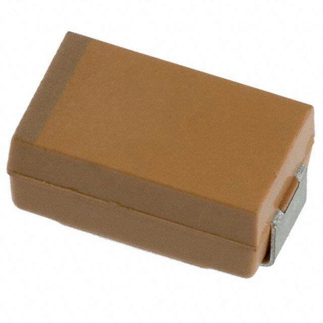
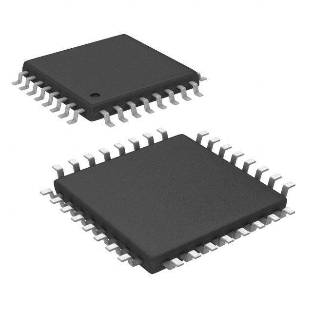

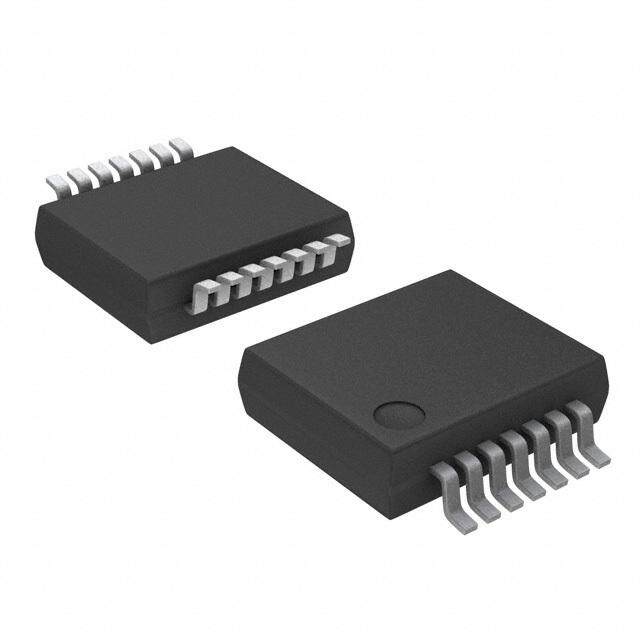

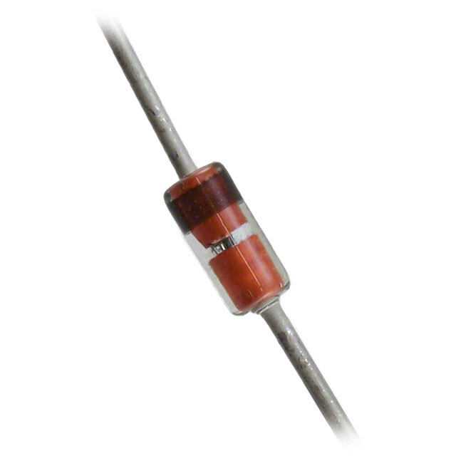
PDF Datasheet 数据手册内容提取
MAX15006/MAX15007 40V, Ultra-Low Quiescent-Current Linear Regulators in 6-Pin TDFN/8-Pin SO General Description Features The MAX15006/MAX15007 ultra-low quiescent-current ● Wide Operating Input Voltage Range (4V to 40V) linear regulators are ideal for use in automotive and ● Guaranteed 50mA Output Current battery-operated systems. These devices operate from an ● Low Quiescent Current input voltage of 4V to 40V, deliver up to 50mA of output 10μA (No Load) and 90μA (Full Load) current, and consume only 10μA of quiescent current at ● Operates Through Cold-Crank Condition no load. The internal p-channel pass device keeps the ● Withstands 45V Load Dump quiescent current low even at full load. The MAX15007 ● Low Dropout Voltage of 300mV consumes only 3μA current when in shutdown. (MAX15006B/MAX15007B) The MAX15006A/MAX15007A have a fixed 3.3V output ● Stable Operation with Tiny 2.2μF Output Capacitor while the MAX15006B/MAX15007B have a fixed 5V ● Enable Input (MAX15007) output voltage. The MAX15006C/MAX15007C feature ● Preset 3.3V and 5.0V Output Voltages an adjustable output from 1.8V to 10V. The MAX15007 includes an enable input to turn the device on or off. All ● 1.8V to 10V Adjustable Output (MAX15006C/ devices are short-circuit protected and include thermal MAX15007C) shutdown. ● Thermal and Short-Circuit Protection ● -40°C to +125°C Operating Temperature Range The MAX15006/MAX15007 operate over the -40°C to +125°C automotive temperature range. These devices ● Thermally Enhanced 3mm x 3mm 6-Pin TDFN/ are available in space-saving 3mm x 3mm 6-pin TDFN 8-Pin SO Packages and 8-pin SO thermally enhanced packages. Ordering Information Applications PIN- TOP PART TEMP RANGE ● Automotive PACKAGE MARK ● Tire-Pressure Monitoring MAX15006AASA+ -40°C to +125°C 8 SO-EP* — ● Industrial MAX15006AASA/V+ -40°C to +125°C 8 SO-EP* — ● Telecom MAX15006AATT+ -40°C to +125°C 6 TDFN-EP* APE ● Networking MAX15006AATT/V+ -40°C to +125°C 6 TDFN-EP* AUR +Denotes a lead(Pb)-free/RoHS-compliant package. /V denotes an automotive qualified part. *EP = Exposed pad. Ordering Information continued at end of data sheet. Pin Configurations TOP VIEW OUT OUT (FB) GND 6 5 4 + MAX15006A IN 1 8 OUT MAX15006B MAX15006A MAX15006C N.C. 2 MAX15006B 7 N.C. (FB) MAX15006C N.C. 3 6 N.C. + EP N.C. 4 EP 5 GND 1 2 3 SO IN IN N.C. TDFN ( ) FOR MAX15006C ONLY. Pin Configurations continued at end of data sheet. 19-0663; Rev 8; 3/15
MAX15006/MAX15007 40V, Ultra-Low Quiescent-Current Linear Regulators in 6-Pin TDFN/8-Pin SO Absolute Maximum Ratings IN to GND ..............................................................-0.3V to +45V Operating Temperature Range .........................-40°C to +125°C EN to GND ............................................................-0.3V to +45V Junction Temperature ......................................................+150°C OUT, FB to GND ...................................................-0.3V to +12V Storage Temperature Range ............................-65°C to +150°C OUT Short-Circuit Duration .......................................Continuous Lead Temperature (soldering, 10s) .................................+300°C Maximum Current Into Any Pin (except IN and OUT) ......±50mA Soldering Temperature (reflow) .......................................+260°C Continuous Power Dissipation (TA = +70°C) TDFN (derate 23.8mW/°C above +70°C) ..................1904mW SO (derate 18.90mW/°C above +70°C) ...............1509.40mW Stresses beyond those listed under “Absolute Maximum Ratings” may cause permanent damage to the device. These are stress ratings only, and functional operation of the device at these or any other conditions beyond those indicated in the operational sections of the specifications is not implied. Exposure to absolute maximum rating conditions for extended periods may affect device reliability. Package Thermal Characteristics (Note 1) TDFN SO Junction-to-Ambient Thermal Resistance (θJA) ..........42°C/W Junction-to-Ambient Thermal Resistance (θJA) ..........53°C/W Junction-to-Case Thermal Resistance (θJC) .................9°C/W Junction-to-Case Thermal Resistance (θJC) .................7°C/W Note 1: Package thermal resistances were obtained using the method described in JEDEC specification JESD51-7, using a four-layer board. For detailed information on package thermal considerations, refer to www.maximintegrated.com/thermal-tutorial. Electrical Characteristics (VIN = 14V, IOUT = 1mA, CIN = 0.1μF, COUT = 2.2μF, TA = TJ = -40°C to +125°C, unless otherwise noted. Typical specifications are a TA = +25°C.) (Note 2) PARAMETER SYMBOL CONDITIONS MIN TYP MAX UNITS Input Voltage Range VIN 4 40 V IOUT = 0A (MAX15006A/B/D) 10 17 IOUT = 0A (MAX15006C) 8 15 IOUT = 0A (MAX15007A/B) 11 18 IOUT = 0A (MAX15007C) 9 16 IOUT = 100µA (MAX15006A/ 10.5 18 B/D) IOUT = 100µA (MAX15006C) 8.5 16 Regulator on, IOUT = 100µA (MAX15007A/B) 11.5 19 Ground Current IGND measured at GND IOUT = 100µA (MAX15007C) 9.5 17 µA IOUT = 1mA (MAX15006A/B/D) 12 20 IOUT = 1mA (MAX15006C) 10 18 IOUT = 1mA (MAX15007A/B) 13 21 IOUT = 1mA (MAX15007C) 11 19 IOUT = 50mA (MAX15006) 90 150 IOUT = 50mA (MAX15007) 93 150 IOUT = 60mA (MAX15006D) 110 150 Shutdown Supply Current ISHDN Regulator off (MAX15007 only) 3 5 µA www.maximintegrated.com Maxim Integrated │ 2
MAX15006/MAX15007 40V, Ultra-Low Quiescent-Current Linear Regulators in 6-Pin TDFN/8-Pin SO Electrical Characteristics (continued) (VIN = 14V, IOUT = 1mA, CIN = 0.1μF, COUT = 2.2μF, TA = TJ = -40°C to +125°C, unless otherwise noted. Typical specifications are a TA = +25°C.) (Note 2) PARAMETER SYMBOL CONDITIONS MIN TYP MAX UNITS REGULATOR VIN ≥ VOUT + ∆VDO 50 Guaranteed Output Current IOUT mA VIN ≥ VOUT + ∆VDO (MAX15006D only) 60 MAX15006A/D, MAX15007A 3.25 3.3 3.35 Output Voltage (Note 3) VOUT IOUT = 1mA MAX15006B/MAX15007B 4.925 5.0 5.075 V MAX15006C/MAX15007C 1.8 10 IOUT = 5mA, MAX15006B/MAX15007B 30 53 IOUT = 5mA, MAX15006C/MAX15007C 30 60 IOUT = 50mA, MAX15006B/MAX15007B 300 525 Dropout Voltage (Notes 4, 5) ∆VDO mV IOUT = 50mA, MAX15006C/MAX15007C 300 600 IOUT = 50mA, MAX15006A/MAX15007A 1000 IOUT = 60mA, MAX15006D 1000 Line Regulation 6V ≤ VIN ≤ 35V, IOUT = 1mA 0.25 % VIN = VOUT + 3V, IOUT = 100µA to 50mA 0.7 1.5 Load Regulation VIN = VOUT + 3V, IOUT = 100µA to 60mA 0.7 1.5 % (MAX15006D) Output Current Limit 80 350 mA Output Voltage Noise 15000mHAz, tCoO 1U0T0 k=H 2z.,2 IµOFUT = VVOOUUTT == 35.V3V 111759 µVRMS Power-Supply Rejection Ratio PSRR f = 100Hz, VIN_RIPPLE = 500mVP-P, IOUT = 50mA 66 dB FB Threshold Voltage VFB ILOAD = 1mA (MAX15006C/MAX15007C only) 1.2 1.23 1.26 V FB Input Current IFB VFB = 0V, 1.5V (MAX15006C/MAX15007C only) -100 +100 nA ENABLE LOGIC VIL 0.4 Enable Threshold Voltage V VIH 1.4 Enable Threshold Hysteresis 60 mV Enable Pulldown Current Internally pulled down to GND 0.5 µA Enable to Regulation Time (Note 6) 0.4 2 ms THERMAL SHUTDOWN Thermal Shutdown TSHDN Junction temperature rising +165 °C Thermal Shutdown Hysteresis THYST 20 °C Note 2: Limits at TA = -40°C are guaranteed by design. Note 3: Output voltage regulation is guaranteed for IOUT ≥ 5μA. Note 4: Dropout voltage is defined as (VIN - VOUT) when VOUT is 2% below the value of VOUT when VIN = VOUT + 3V. Note 5: For VOUT = 3.3V, the 700mV dropout indicates VOUT does not reach 2% below VOUT at VIN = VOUT + 3V at minimum 4V input voltage. Note 6: Enable to regulation time is the time the output takes to reach 95% of its final value with VIN = 14V and EN is taken from VIL to VIH in 5ns. www.maximintegrated.com Maxim Integrated │ 3
MAX15006/MAX15007 40V, Ultra-Low Quiescent-Current Linear Regulators in 6-Pin TDFN/8-Pin SO Typical Operating Characteristics (VIN = 14V, CIN = 0.1μF, COUT = 2.2μF, VEN = VIN, TA = +25°C, unless otherwise noted.) OUTPUT VOLTAGE vs. INPUT VOLTAGE OUTPUT VOLTAGE vs. INPUT VOLTAGE OUTPUT VOLTAGE vs. TEMPERATURE (MAX15006A/MAX15007A) (MAX15006B/MAX15007B) (MAX15006A/MAX15007A) 333...036 MAX15006 toc01 455...505 MAX15006 toc02 333...344925 MAX15006 toc03 2.7 4.0 IOUT = 1mA 3.36 2.4 3.5 V) 2.1 V) V)3.33 (UT 1.8 (UT 3.0 (UT3.30 VO 1.5 VO 2.5 VO3.27 2.0 1.2 3.24 0.9 1.5 IOUT = 50mA 0.6 1.0 3.21 0.3 IOUT = 0 0.5 IOUT = 0 3.18 0 0 3.15 0 5 10 15 20 25 30 35 40 0 5 10 15 20 25 30 35 40 -50 -25 0 25 50 75 100 125 150 VIN (V) VIN (V) TEMPERATURE (°C) OUTPUT VOLTAGE vs. TEMPERATURE DROPOUT VOLTAGE vs. LOAD CURRENT GROUND CURRENT vs. LOAD CURRENT (MAX15006B/MAX15007B) (MAX15006B/MAX15007B) (MAX15006B/MAX15007B) 5555....11220505 IOUT = 1mA MAX15006 toc04 V) 344550500000 TA T=A + =2 5+C125C MAX15006 toc05 178900000 TA = +125°C MAX15006 toc06 V (V)OUT455...900505 (mDROPOUT 223050000 TA = -40C I (A)GND 456000 TA = +25°C V 4.90 IOUT = 50mA 150 30 TA = -40°C 4.85 100 20 4.80 50 10 4.75 0 0 -50 -25 0 25 50 75 100 125 150 0 5 10 15 20 25 30 35 40 45 50 0 5 10 15 20 25 30 35 40 45 50 TEMPERATURE (°C) IOUT (mA) IOUT (mA) GROUND CURRENT vs. TEMPERATURE GROUND CURRENT vs. TEMPERATURE SHUTDOWN SUPPLY CURRENT (IOUT = 0) (IOUT = 50mA) vs. TEMPERATURE 111468 MAX15006 toc07 1990890 MAX15006 toc08 1890 VIN = +40V MAX15006 toc09 97 7 12 I (A)GND 180 VIN = +14V VIN = +40V I (A)GND 999456 I (A)SHDN 456 VIN = +14VVIN = +6V 6 VIN = +6V 93 3 4 92 2 2 91 1 0 90 0 -50 -25 0 25 50 75 100 125 150 -50 -25 0 25 50 75 100 125 150 -50 -25 0 25 50 75 100 125 150 TEMPERATURE (°C) TEMPERATURE (°C) TEMPERATURE (°C) www.maximintegrated.com Maxim Integrated │ 4
MAX15006/MAX15007 40V, Ultra-Low Quiescent-Current Linear Regulators in 6-Pin TDFN/8-Pin SO Typical Operating Characteristics (continued) (VIN = 14V, CIN = 0.1μF, COUT = 2.2μF, VEN = VIN, TA = +25°C, unless otherwise noted.) GROUND CURRENT DISTRIBUTION GROUND CURRENT DISTRIBUTION GROUND CURRENT DISTRIBUTION (TA = -40°C) (TA = +25°C) (TA = +125°C) 222147 5M0A UXN15IT0S0 7T, EIOSUTTE =D 0 MAX15006 toc10 222147 5M0A UXN15IT0S0 7T, EIOSUTTE =D 0 MAX15006 toc11 222147 5M0A UXN15IT0S0 7T, EIOSUTTE =D 0 MAX15006 toc12 S S S NIT 18 NIT 18 NIT 18 U U U F 15 F 15 F 15 O O O R R R E 12 E 12 E 12 B B B M M M NU 9 NU 9 NU 9 6 6 6 3 3 3 0 0 0 10.4 10.5 10.6 10.7 10.8 10.9 11.0 10.8 10.9 11.0 11.1 11.2 11.3 11.4 11.6 11.7 11.8 11.9 12.0 12.1 IGND (µA) IGND (µA) IGND (µA) LOAD-TRANSIENT RESPONSE INPUT-VOLTAGE STEP RESPONSE STARTUP RESPONSE (MAX15006B/MAX15007B) (MAX15006B/MAX15007B, IOUT = 1mA) MAX15006 toc15 MAX15006 toc13 MAX15006 toc14 VOUT 18V VIN AC-COUPLED VIN 5V/div 200mV/div 14V 50mA IOUT VOUT VOUT 1mA AC-COUPLED 2V/div 100mV/div MAX15006B/MAX15007B IOUT = 1mA 200µs/div 400µs/div 400µs/div ENABLE STARTUP RESPONSE ENABLE STARTUP RESPONSE ENABLE STARTUP RESPONSE MAX15006 toc16 MAX15006 toc17 MAX15006 toc18 EN EN EN 1V/div 1V/div 1V/div VOUT VOUT VOUT 2V/div 2V/div 2V/div MAX15006B/MAX15007B MAX15006B/MAX15007B MAX15006B/MAX15007B IOUT = 0 IOUT = 50mA VIN = 40V, IOUT = 0 400µs/div 400µs/div 400µs/div www.maximintegrated.com Maxim Integrated │ 5
MAX15006/MAX15007 40V, Ultra-Low Quiescent-Current Linear Regulators in 6-Pin TDFN/8-Pin SO Typical Operating Characteristics (continued) (VIN = 14V, CIN = 0.1μF, COUT = 2.2μF, VEN = VIN, TA = +25°C, unless otherwise noted.) POWER-SUPPLY REJECTION RATIO OUTPUT-NOISE SPECTRAL DENSITY ENABLE STARTUP RESPONSE vs. FREQUENCY vs. FREQUENCY MAX15006 toc19 EN --21000 IOUT = 50mA MAX15006 toc20 TY (µV/√Hz) 10 MAX15006 toc21 1V/div -30 COUT = 2.2µF NSI E 1 D B) -40 L d A RR ( -50 CTR S E P -60 SP E 0.1 VOUT -70 OIS 2V/div N -80 COUT = 10µF T- MVIANX =1 4500V06, BIO/MUTA =X 15500m0A7B -90 UTPU MIOAUXT 1=5 5000m6AA/MAX15007A O -100 0.01 400µs/div 0.01 0.1 1 10 100 1000 0.01 0.1 1 10 100 FREQUENCY (kHz) FREQUENCY (kHz) OUTPUT-NOISE SPECTRAL DENSITY OUTPUT VOLTAGE NOISE vs. FREQUENCY vs. LOAD CURRENT TY (µV/√Hz) 10 MAX15006 toc22 111235050 MAX15006 toc23 NSI 105 E 1 PECTRAL D e (µV)nRMS 679050 S E 0.1 S 45 OI T-N 30 UTPU MIOAUXT 1=5 5000m6BA/MAX15007B 15 MAX15006A/MAX15007A O0.01 0 0.01 0.1 1 10 100 0 5 10 15 20 25 30 35 40 45 50 FREQUENCY (kHz) IOUT (mA) FB VOLTAGE vs. INPUT VOLTAGE FB VOLTAGE vs. TEMPERATURE (MAX15007C, VOUT = 5V) (MAX15007C, VOUT = 5V) 11..222390 MAX15006 toc24 111...222223890 MAX15006 toc25 1.227 1.228 1.226 V) V) (B (B1.225 VF VF 1.227 1.224 1.223 1.226 1.222 1.221 1.225 1.220 5 10 15 20 25 30 35 40 -50 -25 0 25 50 75 100 125 150 VIN (V) TEMPERATURE (°C) www.maximintegrated.com Maxim Integrated │ 6
MAX15006/MAX15007 40V, Ultra-Low Quiescent-Current Linear Regulators in 6-Pin TDFN/8-Pin SO Typical Operating Characteristics (continued) (VIN = 14V, CIN = 0.1μF, COUT = 2.2μF, VEN = VIN, TA = +25°C, unless otherwise noted.) OUTPUT VOLTAGE NOISE CLAMPED LOAD DUMP vs. OUTPUT CAPACITANCE (IOUT = 0) 111235050 MAX15006 toc26 MAX15006 toc27 40V VIN 105 )S 90 M R 13.5V µV 75 e (n 60 45 VOUT AC-COUPLED 30 20mV/div MAX15006A/MAX15007A 15 IOUT = 25mA 0 0 2 4 6 8 10 12 14 16 18 20 22 100ms/div COUT (µF) Pin Description PIN MAX15006A/B MAX15006C MAX15007A/B MAX15007C NAME FUNCTION TDFN SO TDFN SO TDFN SO TDFN SO Regulator Supply Input. Supply voltage ranges 1, 2 1 1, 2 1 1, 2 1 1, 2 1 IN from 4V to 40V. Bypass with a 0.1µF capacitor to GND. 2, 3, 2, 3, 2, 4, 3 3 — — 2, 4, 6 N.C. No Connection. Not internally connected. 4, 6, 7 4, 6 6, 7 4 5 4 5 4 5 4 5 GND Ground Regulator Output. Bypass OUT to GND with a 5, 6 8 6 8 5, 6 8 6 8 OUT low-ESR capacitor with a minimum 2.2µF. Feedback Regulation Set-Point. Connect an external resistive divider network from OUT to FB — — 5 7 — — 5 7 FB to GND to adjust the output voltage from 1.8V to 10V. Active-High Enable Input. Force EN high (or connect to VIN) to turn the regulator on. Pull EN low (or leave unconnected) to place the device — — — — 3 3 3 3 EN in a low-power shutdown mode. EN is internally pulled down to GND through a 0.5µA sink current. Exposed Pad. Internally connected to GND. Connect EP to the ground plane for enhanced — — — — — — — — EP thermal performance. Do not use EP as a ground connection. www.maximintegrated.com Maxim Integrated │ 7
MAX15006/MAX15007 40V, Ultra-Low Quiescent-Current Linear Regulators in 6-Pin TDFN/8-Pin SO Functional Diagrams IN - FET DRIVER WITH + CURRENT LIMIT OUT ERROR THERMAL 1.242V AMPLIFIER SENSOR REF FB (FOR MAX15006C ONLY) GND MAX15006 (FOR MAX15006A/B ONLY) Figure 1. MAX15006 Simplified Functional Diagram IN CONTROL EN - FET DRIVER LOGIC WITH + CURRENT LIMIT OUT ERROR THERMAL 1.242V AMPLIFIER SENSOR REF FB (FOR MAX15007C ONLY) GND MAX15007 (FOR MAX150076A/B ONLY) Figure 2. MAX15007 Simplified Functional Diagram www.maximintegrated.com Maxim Integrated │ 8
MAX15006/MAX15007 40V, Ultra-Low Quiescent-Current Linear Regulators in 6-Pin TDFN/8-Pin SO Detailed Description EN Input (MAX15007 Only) The MAX15006/MAX15007 high-voltage linear regula- EN is an active-high, logic-level enable input that turns tors operate over a 4V to 40V input voltage range. These the device on or off. Drive EN high to turn the device on. devices guarantee 50mA load drive, and offer preset An internal 0.5μA pulldown current keeps the MAX15007 output voltages of +3.3V (MAX15006A/MAX15007A) or in shutdown mode when driven by a three-state driver +5V (MAX15006B/MAX15007B) or an adjustable voltage in high-impedance mode, or an open-drain driver. While output from 1.8V to 10V (MAX15006C/MAX15007C). in shutdown, the device consumes only 3μA (typ). EN Thermal shutdown and short-circuit protection prevent withstands voltages up to 40V, allowing it to be driven by damage during overtemperature and overcurrent condi- high input level voltages or connected to IN for always-on tions. The MAX15007 includes an enable input (EN) operation. allowing the regulators to be turned on/off using a logic- Thermal Protection level voltage. Driving EN high turns on the device while When the junction temperature exceeds +165°C, an driving EN low places the device in a low-power shutdown internal thermal sensor turns the pass transistor off, and mode. In shutdown, the supply current is reduced to 3μA allows the device to cool. The thermal sensor turns the (typ). The MAX15006/MAX15007 operate over the -40°C pass transistor on again after the junction temperature to +125°C automotive temperature range. All devices are cools by 20°C. This results in a cycled output during con- available in thermally enhanced 6-pin TDFN and 8-pin SO tinuous thermal-overload conditions. Thermal protection packages capable of dissipating 1.904W and 1.509W at protects the MAX15006/MAX15007 in the event of fault TA = +70°C, respectively. conditions. Operation at TJ = +150°C without going into Regulator thermal shutdown is not guaranteed. Use Figures 3a and The regulator accepts an input voltage from 4V to 40V. 3b to determine the minimum guaranteed output current. The MAX15006A/MAX15007A have a fixed 3.3V output Output Short-Circuit Current Limit voltage while the MAX15006B/MAX15007B offer a fixed The MAX15006/MAX15007 feature a 175mA current limit. 5V output voltage. The MAX15006C/MAX15007C feature The output can be shorted to GND for an indefinite period an adjustable voltage output by connecting an external of time without damage to the device. During a short resistive divider from OUT to FB and to GND (see the circuit, the power dissipated across the pass transistor Output Voltage Setting section). can quickly heat the device. When the die temperature reaches +165°C, the MAX15006/MAX15007 shut down mA) 44550505 VIN = 18VVIN, V=O 1U8TV =, 5V MAX15006 fig03a mA) 44550505 VIN = 18VVI,N V =O U18T V=, 5V MAX15006 fig03b NT ( 35 VOUT = 3.3V NT ( 35 VOUT = 3.3V E E RR 30 RR 30 U U UT C 25 VIN = 26V, VOUT = 5V UT C 25 VIN = 26V, VOUT = 5V P 20 P 20 T T U U O 15 O 15 10 VIN = 26V, VOUT = 3.3V 10 VIN = 26V, VOUT = 3.3V 5 5 0 0 80 85 90 95 100 105 110 115 120 125 130 80 85 90 95 100 105 110 115 120 125 130 AMBIENT TEMPERATURE (°C) AMBIENT TEMPERATURE (°C) Figure 3a. Minimum Output Current vs. Ambient Temperature Figure 3b. Minimum Output Current vs. Ambient Temperature (6-Pin TDFN-EP) (8-Pin SO-EP) www.maximintegrated.com Maxim Integrated │ 9
MAX15006/MAX15007 40V, Ultra-Low Quiescent-Current Linear Regulators in 6-Pin TDFN/8-Pin SO and automatically restart after the die temperature cools 1.9048W for TA ≤ +70°C by 20°C. PD = 1.9048W − 0.0238W × (TA–70°C) for +70°C < TA ≤ +125°C °C Applications Information Output Voltage Setting For the SO-EP package: The MAX15006C/MAX15007C provide an adjustable output voltage from 1.8V to 10V and do not operate in a 1.8605W for TA ≤ +70°C preset output voltage mode. Connect an external resis- PD = 1.8605W − 0.0233W × (TA–70°C) for +70°C < TA ≤ +125°C tive divider from OUT to FB to GND as shown in Figure 4 °C to set the desired output voltage. VOUT is calculated as After determining the allowable package dissipation, follows: calculate the maximum allowable output current, without R1 VOUT =VFB×1+ exceeding the +150°C junction temperature, using the R2 following formula: where VFB = 1.23V and a 5μA minimum current is P required in the external divider for stability. I = D ≤ 50mA OUT(MAX) V −V IN OUT Available Output Current Calculation The above equations do not include the negligible power The MAX15006/MAX15007 provide up to 50mA of con- dissipation from self-heating due to the IC ground current. tinuous output current. The input voltage range extends to 40V. Package power dissipation limits the amount of Example 1 (TDFN Package): output current available for a given input/output voltage TA = +125°C and ambient temperature. Figure 5 shows the maximum allowable power dissipation for these devices to keep the VIN = 26V junction temperature below +150°C. Figure 5 assumes VOUT = 3.3V that the exposed metal pad of the MAX15006/MAX15007 Calculate the maximum allowable package dissipation at is soldered to 1in2 of PCB copper. the given temperature as follows: Use Figure 5 to determine the allowable package dissipa- W tion for a given ambient temperature. Alternately, use the P = 1.9048W − 0.0238 (125°C − 70°C) = 595.8mW D following formulas to calculate the allowable package dis- °C sipation. For the TDFN package: +40V. 1TµOF +40V IN OUT R1 +1.8V TO 2+.21µ0VF 222...024 1(6.9-P4I0N8 WTDFN) MAX15006 fig04 MAX15007C 1.8 DERATE 1.8605W 1.6 (8-PIN SO-EP) 23.8mW/C FB W) 1.4 ON (D 1.2 P DERATE OFF EN 1.0 23.3mW/C R2 0.8 GND 0.6 0.4 0.2 0 0 20 40 60 80 100 120 140 VOUT = VFB (1 + R1/R2) VFB = 1.23V TEMPERATURE (°C) Figure 4. Setting the Adjustable Output Voltage Figure 5. Calculated Maximum Power Dissipation vs. Ambient Temperature www.maximintegrated.com Maxim Integrated │ 10
MAX15006/MAX15007 40V, Ultra-Low Quiescent-Current Linear Regulators in 6-Pin TDFN/8-Pin SO And establish the maximum output current: Find the maximum output current: 595.8mW 1.9048W IOUT(MAX) = = 26.2mA IOUT(MAX) = = 476mA ⇒ IOUT(MAX) = 50mA 26V−3.3V 9V−5V Example 2 (TDFN Package): In Examples 2 and 3, the maximum output current is cal- culated as 172mA and 476mA, respectively; however, the TA = +85°C allowable output current cannot exceed 50mA. VIN = 14V Alternately, use Figures 6a and 6b to quickly determine VOUT = 5V the maximum allowable output current for selected ambi- Calculate the maximum allowable package dissipation at ent temperatures and input voltages. the given temperature as follows: Output-Capacitor Selection W and Regulator Stability P = 1.9048W − 0.0238 (85°C − 70°C) = 1.5478W D °C For stable operation over the full temperature range and with load currents up to 50mA, use a low-ESR 2.2μF (min) Then determine the maximum output current: ceramic or tantalum output capacitor. Use larger output- capacitor values such as 22μF to reduce noise, improve 1.5478W IOUT(MAX) = = 172mA ⇒ IOUT(MAX) = 50mA load-transient response, and power-supply rejection. 14V−5V Some ceramic dielectrics exhibit large capacitance and Example 3 (TDFN Package): ESR variations with temperature. Ensure the minimum capacitance under worst-case conditions does not drop TA = +50°C below 1.3μF to ensure output stability. With an X7R VIN = 9V dielectric, 2.2μF should be sufficient at all operating tem- VOUT = 5V peratures. Calculate the maximum allowable package dissipation at the given temperature as follows: PD = 1.9048W 45565050 MAX15006 fig05a 45565050 MAX15006 fig05b TA = +70°C TA = +70°C A) 40 A) 40 m m (X) 35 TA = +85°C (X) 35 TA = +85°C MA 30 MA 30 OUT( 25 TA = +125°C OUT( 25 TA = +125°C I 20 I 20 15 15 10 10 5 VOUT = 5V 5 VOUT = 5V 6-PIN TDFN 8-PIN SO-EP 0 0 0 5 10 15 20 25 30 35 40 0 5 10 15 20 25 30 35 40 VIN (V) VIN (V) Figure 6a. Calculated Maximum Output Current vs. Input Figure 6b. Calculated Maximum Output Current vs. Input Voltage (6-Pin TDFN-EP) Voltage (8-Pin SO-EP) www.maximintegrated.com Maxim Integrated │ 11
MAX15006/MAX15007 40V, Ultra-Low Quiescent-Current Linear Regulators in 6-Pin TDFN/8-Pin SO Selector Guide FIXED OUTPUT ADJUSTABLE OUTPUT PART ENABLE INPUT PIN-PACKAGE VOLTAGE (V) VOLTAGE (V) MAX15006AASA+ — 3.3 — 8 SO-EP MAX15006AATT+ — 3.3 — 6 TDFN-EP MAX15006BASA+ — 5 — 8 SO-EP MAX15006BATT+ — 5 — 6 TDFN-EP MAX15006CASA+ — — ADJ (1.8 to 10) 8 SO-EP MAX15006CATT+ — — ADJ (1.8 to 10) 6 TDFN-EP MAX15007AASA+ √ 3.3 — 8 SO-EP MAX15007AATT+ √ 3.3 — 6 TDFN-EP MAX15007BASA+ √ 5 — 8 SO-EP MAX15007BATT+ √ 5 — 6 TDFN-EP MAX15007CASA+ √ — ADJ (1.8 to 10) 8 SO-EP MAX15007CATT+ √ — ADJ (1.8 to 10) 6 TDFN-EP Pin Configurations (continued) TOP VIEW OUT OUT (FB) GND 6 5 4 + IN 1 8 OUT MAX15007A MAX15007A MAX15007B N.C. 2 MAX15007B 7 N.C. (FB) MAX15007C MAX15007C EN 3 6 N.C. N.C. 4 EP 5 GND + EP SO 1 2 3 IN IN EN TDFN ( ) FOR MAX15007C ONLY. www.maximintegrated.com Maxim Integrated │ 12
MAX15006/MAX15007 40V, Ultra-Low Quiescent-Current Linear Regulators in 6-Pin TDFN/8-Pin SO Ordering Information (continued) Chip Information PROCESS: BiCMOS PIN- TOP PART TEMP RANGE PACKAGE MARK MAX15006BASA+ -40°C to +125°C 8 SO-EP* — Package Information MAX15006BASA/V+ -40°C to +125°C 8 SO-EP* — For the latest package outline information and land patterns MAX15006BATT+ -40°C to +125°C 6 TDFN-EP* APF (footprints), go to www.maximintegrated.com/packages. Note MAX15006BATT/V+ -40°C to +125°C 6 TDFN-EP* AUN that a “+”, “#”, or “-” in the package code indicates RoHS status MAX15006CATT+ -40°C to +125°C 6 TDFN-EP* API only. Package drawings may show a different suffix character, but MAX15006CATT/V+ -40°C to +125°C 6 TDFN-EP* AVA the drawing pertains to the package regardless of RoHS status. MAX15006DATT/V+ -40°C to +125°C 6 TDFN-EP* AVL PACKAGE PACKAGE OUTLINE LAND MAX15007AASA+ -40°C to +125°C 8 SO-EP* — TYPE CODE NO. PATTERN NO. MAX15007AATT+ -40°C to +125°C 6 TDFN-EP* APG 6 TDFN-EP T633+2 21-0137 90-0058 MAX15007BASA+ -40°C to +125°C 8 SO-EP* — 8 SO-EP S8E+12 21-0111 90-0150 MAX15007BATT+ -40°C to +125°C 6 TDFN-EP* APH MAX15007BATT/V+ -40°C to +125°C 6 TDFN-EP* AVK MAX15007CATT+ -40°C to +125°C 6 TDFN-EP* APJ MAX15007CATT/V+ -40°C to +125°C 6 TDFN-EP* AUU +Denotes a lead(Pb)-free/RoHS-compliant package. /V denotes an automotive qualified part. *EP = Exposed pad. www.maximintegrated.com Maxim Integrated │ 13
MAX15006/MAX15007 40V, Ultra-Low Quiescent-Current Linear Regulators in 6-Pin TDFN/8-Pin SO Revision History REVISION REVISION PAGES DESCRIPTION NUMBER DATE CHANGED 0 10/06 Initial release — Added MAX15006C/MAX15007C adjustable version to data sheet including Ordering 1 5/08 1–14 Information, Electrical Characteristics, Pin Description, and Detailed Description 2 11/09 Added the MAX15006A/MAX15006B automotive packages to the Ordering Information 1, 13 Added the MAX15006CATT and MAX15007CATT automotive packages to the Ordering 3 12/10 13 Information Added the MAX15006AASA and MAX15006BASA automotive packages to the Ordering 4 7/11 1, 13 Information 5 11/11 Changed the maximum IOUT = 50mA dropout of the MAX15006A/MAX15007A from 3 700mV to 1000mV 6 1/13 Added MAX15006DATT/V and MAX15007BATT/V 1–14 7 8/14 Corrected thermal resistance data in Package Thermal Characteristics section 2 8 3/15 Corrected continuous power dissipation for SO package in Absolute Maximum Ratings 2 For pricing, delivery, and ordering information, please contact Maxim Direct at 1-888-629-4642, or visit Maxim Integrated’s website at www.maximintegrated.com. Maxim Integrated cannot assume responsibility for use of any circuitry other than circuitry entirely embodied in a Maxim Integrated product. No circuit patent licenses are implied. Maxim Integrated reserves the right to change the circuitry and specifications without notice at any time. The parametric values (min and max limits) shown in the Electrical Characteristics table are guaranteed. Other parametric values quoted in this data sheet are provided for guidance. Maxim Integrated and the Maxim Integrated logo are trademarks of Maxim Integrated Products, Inc. © 2015 Maxim Integrated Products, Inc. │ 14
Mouser Electronics Authorized Distributor Click to View Pricing, Inventory, Delivery & Lifecycle Information: M axim Integrated: MAX15006AASA+ MAX15006BASA+ MAX15007AASA+ MAX15007BASA+ MAX15007CATT/V+T MAX15006CATT/V+T MAX15006BASA/V+ MAX15006BASA/V+T MAX15006AASA+T MAX15006AATT+T MAX15006AATT/V+T MAX15006BASA+T MAX15006BATT+T MAX15006CATT+T MAX15007AASA+T MAX15007AATT+T MAX15007BASA+T MAX15007BATT+T MAX15007CATT+T MAX15006BATT/V+T MAX15007AATT+TW MAX15007BATT/V+