ICGOO在线商城 > MAX16055GAUB+

 Datasheet下载
- 型号: MAX16055GAUB+
- 制造商: Maxim
- 库位|库存: xxxx|xxxx
- 要求:
| 数量阶梯 | 香港交货 | 国内含税 |
| +xxxx | $xxxx | ¥xxxx |
查看当月历史价格
查看今年历史价格
MAX16055GAUB+产品简介:
ICGOO电子元器件商城为您提供MAX16055GAUB+由Maxim设计生产,在icgoo商城现货销售,并且可以通过原厂、代理商等渠道进行代购。 提供MAX16055GAUB+价格参考¥26.01-¥26.01以及MaximMAX16055GAUB+封装/规格参数等产品信息。 你可以下载MAX16055GAUB+参考资料、Datasheet数据手册功能说明书, 资料中有MAX16055GAUB+详细功能的应用电路图电压和使用方法及教程。
| 参数 | 数值 |
| 产品目录 | 集成电路 (IC)半导体 |
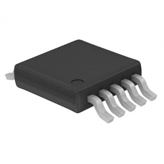
| 描述 | IC MPU SUPERVISOR HEX 10MSOP监控电路 Hex Voltage MPU Supervisor |
| 产品分类 | |
| 品牌 | Maxim Integrated |
| 产品手册 | |
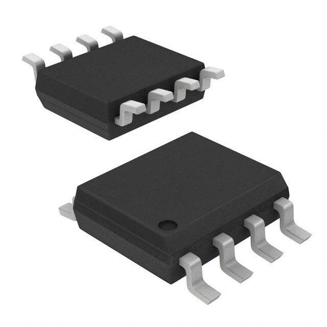
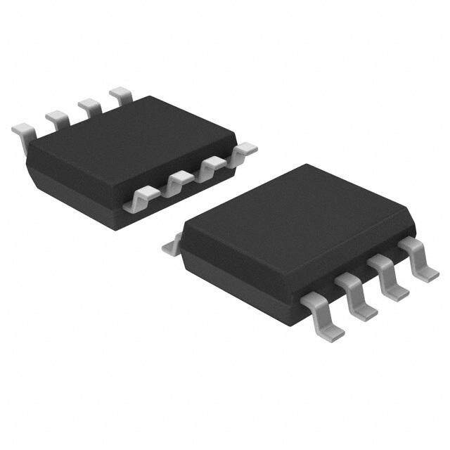
| 产品图片 |
|
| rohs | 符合RoHS无铅 / 符合限制有害物质指令(RoHS)规范要求 |
| 产品系列 | 电源管理 IC,监控电路,Maxim Integrated MAX16055GAUB+- |
| NumberofInputsMonitored | 9 Input |
| 数据手册 | |
| 产品型号 | MAX16055GAUB+ |
| 产品培训模块 | http://www.digikey.cn/PTM/IndividualPTM.page?site=cn&lang=zhs&ptm=25703http://www.digikey.cn/PTM/IndividualPTM.page?site=cn&lang=zhs&ptm=25705 |
| 产品种类 | 监控电路 |
| 人工复位 | Manual Reset |
| 供应商器件封装 | 10-uMAX |
| 功率失效检测 | No |
| 包装 | 管件 |
| 受监控电压数 | 6 |
| 商标 | Maxim Integrated |
| 复位 | 低有效 |
| 复位超时 | 最小为 140 ms |
| 安装类型 | 表面贴装 |
| 安装风格 | SMD/SMT |
| 封装 | Tube |
| 封装/外壳 | 10-TFSOP,10-MSOP(0.118",3.00mm 宽) |
| 封装/箱体 | UMAX-10 |
| 工作温度 | -40°C ~ 125°C |
| 工作电源电流 | 25 uA to 55 uA |
| 工厂包装数量 | 50 |
| 应用说明 | |
| 最大功率耗散 | 444 mW |
| 标准包装 | 1 |
| 欠电压阈值 | 0.5 V |
| 电压-阈值 | 6 种可选阀值组合 |
| 电池备用开关 | No Backup |
| 电源电压-最大 | 5.5 V |
| 电源电压-最小 | 1 V |
| 监视器 | No Watchdog |
| 类型 | Voltage Supervisory |
| 系列 | MAX16055 |
| 芯片启用信号 | No Chip Enable |
| 被监测输入数 | 9 Input |
| 输出 | 开路漏极或开路集电极 |
| 输出类型 | Active Low, Open Drain |
| 重置延迟时间 | 20 us |
| 阈值电压 | 0.9 V to 3.3 V |
| 零件号别名 | MAX16055 |







- 商务部:美国ITC正式对集成电路等产品启动337调查
- 曝三星4nm工艺存在良率问题 高通将骁龙8 Gen1或转产台积电
- 太阳诱电将投资9.5亿元在常州建新厂生产MLCC 预计2023年完工
- 英特尔发布欧洲新工厂建设计划 深化IDM 2.0 战略
- 台积电先进制程称霸业界 有大客户加持明年业绩稳了
- 达到5530亿美元!SIA预计今年全球半导体销售额将创下新高
- 英特尔拟将自动驾驶子公司Mobileye上市 估值或超500亿美元
- 三星加码芯片和SET,合并消费电子和移动部门,撤换高东真等 CEO
- 三星电子宣布重大人事变动 还合并消费电子和移动部门
- 海关总署:前11个月进口集成电路产品价值2.52万亿元 增长14.8%



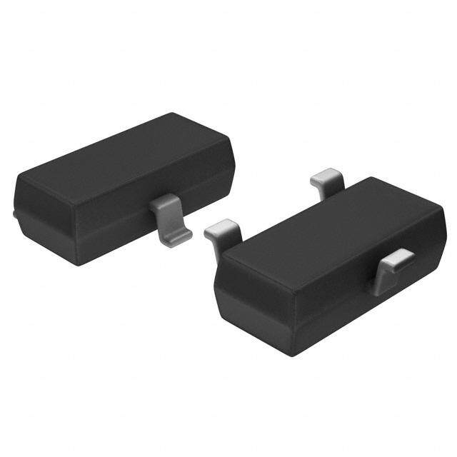
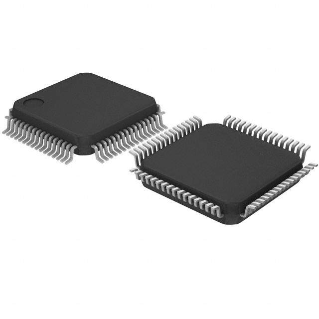
PDF Datasheet 数据手册内容提取
19-4411; Rev 0; 1/09 Ultra-Small, Hex Voltage, Microprocessor Supervisor General Description Features M The MAX16055 precision hex voltage microprocessor ♦ Precision Factory-Set Reset Threshold Options A (µP) supervisory circuit monitors up to six system-sup- 3.3V, 3.0V, 2.5V, 1.8V, 1.5V, 1.2V, 1.1V, 1.0V, and X ply voltages and asserts a single reset when any one 0.9V supply voltage drops below its preset threshold. The 1 device significantly reduces system size and compo- ♦ Adjustable Voltage Threshold Monitors Down to 6 nent count while improving reliability compared to multi- 0.5V with 1.5% Accuracy 0 ple ICs or discrete components. ♦ Open-Drain RESETOutput with 70µA Internal 5 A variety of factory-trimmed threshold voltages are avail- Pullup 5 able to accommodate different supply voltages and tol- erance with minimal external components. The ♦ Fixed 140ms (min) Reset Timeout Period MAX16055 includes internally fixed threshold options for ♦ Manual Reset Input monitoring 3.3V, 3.0V, 2.5V, 1.8V, 1.5V, 1.2V, 1.1V, 1.0V, and 0.9V supplies with -5% or -10% tolerance. The ♦ Reset Valid for IN1 ≥1V or IN2 ≥1V MAX16055 is also available with one to five adjustable ♦ Tolerance Select (5%/10%) Input threshold inputs to monitor voltages down to 0.5V. ♦ Immune to Short Supply Transients A single active-low, open-drain output asserts when any monitored input falls below its associated thresh- old. The reset output features a weak internal pullup Ordering Information (typically 70µA) to supply input IN1. The reset output remains low for the reset timeout period (140ms, min) PART TEMP RANGE PIN-PACKAGE after all voltages rise above the selected thresholds. The reset output remains valid as long as either IN1 or MAX16055_AUB+* -40°C to +125°C 10 µMAX IN2 input voltage is above 1V. The MAX16055 is avail- +Denotes a lead(Pb)-free/RoHS-compliant package. able in a small 10-pin µMAX® (3mm x 3mm) package. *Insert the desired threshold option letter from the Selector The MAX16055 operates over the -40°C to +125°C Guide into the blank to complete the part number. Contact factory automotive temperature range. for availability. Applications Telecommunications Networking Equipment Typical Operating Circuit High-End Printers Industrial Equipment Desktop and Notebook Set-Top Boxes Computers Servers/Workstations Data Storage Equipment MAX16055 µMAX is a registered trademark of Maxim Integrated Products, Inc. Pin Configuration IN1 10kΩ VCC 0.1μF μP RESET MONITORED TOP VIEW SUPPLIES IN2 IN3 IN1 1 + 10 GND IN4 IN5 IN2 2 9 RESET IN6 IN3 3 8 MR MAX16055 MR IN4 4 7 TOL GND TOL IN5 5 6 IN6 μMAX ________________________________________________________________Maxim Integrated Products 1 For pricing, delivery, and ordering information,please contact Maxim Directat 1-888-629-4642, or visit Maxim’s website at www.maxim-ic.com.
Ultra-Small, Hex Voltage, Microprocessor Supervisor 5 ABSOLUTE MAXIMUM RATINGS 5 RESET, TOL, MR, IN_ to GND..................................-0.3V to +6V Operating Temperature Range.........................-40°C to +125°C 0 Input/Output Current (all pins)............................................20mA Storage Temperature Range.............................-65°C to +150°C 6 Continuous Power Dissipation (TA= +70°C) Junction Temperature......................................................+150°C 10-Pin µMAX (derate 5.6mW/°C above +70°C)...........444mW Lead Temperature (soldering, 10s).................................+300°C 1 X Stresses beyond those listed under “Absolute Maximum Ratings” may cause permanent damage to the device. These are stress ratings only, and functional operation of the device at these or any other conditions beyond those indicated in the operational sections of the specifications is not implied. Exposure to A absolute maximum rating conditions for extended periods may affect device reliability. M ELECTRICAL CHARACTERISTICS (VIN1= 1V to 5.5V, TA= -40°C to +125°C, unless otherwise noted. Typical values are at VIN1= 3.3V, TA= +25°C.) (Note 1) PARAMETER SYMBOL CONDITIONS MIN TYP MAX UNIT Operating Voltage Range VIN1 (Note 2) 1.0 5.5 V VIN_ = nominal input voltage (for IN2–IN6; 3.3V, 3.0V, 2.5V, 1.8V, 1.5V, 1.2V, 1.1V, 25 40 1.0V, 0.9V supplies) Input Current (Note 3) IIN_ VIN1 = nominal input voltage (for +3.3V IN1 µA 55 115 supply) VIN_ = 0 to 0.5V or VADJ (for adjustable -0.1 +0.1 thresholds) 3.3V, TOL = GND 3.00 3.08 3.15 3.3V, TOL = VIN1 2.85 2.93 3.00 3.0V, TOL = GND 2.70 2.78 2.85 3.0V, TOL = VIN1 2.55 2.63 2.70 2.5V, TOL = GND 2.25 2.32 2.38 2.5V, TOL = VIN1 2.13 2.19 2.25 1.8V, TOL = GND 1.62 1.67 1.71 1.8V, TOL = VIN1 1.53 1.58 1.62 1.5V, TOL = GND 1.355 1.389 1.425 Threshold Voltage VTH VIN_ decreasing V 1.5V, TOL = VIN1 1.283 1.316 1.350 1.2V, TOL = GND 1.084 1.112 1.140 1.2V, TOL = VIN1 1.027 1.053 1.08 1.1V, TOL = GND 0.993 1.019 1.045 1.1V, TOL = VIN1 0.941 0.965 0.99 1.0V, TOL = GND 0.903 0.926 0.95 1.0V, TOL = VIN1 0.856 0.878 0.90 0.9V, TOL = GND 0.813 0.834 0.855 0.9V, TOL = VIN1 0.770 0.790 0.810 2 _______________________________________________________________________________________
Ultra-Small, Hex Voltage, Microprocessor Supervisor ELECTRICAL CHARACTERISTICS (continued) M (VIN1= 1V to 5.5V, TA= -40°C to +125°C, unless otherwise noted. Typical values are at VIN1= 3.3V, TA= +25°C.) (Note 1) A PARAMETER SYMBOL CONDITIONS MIN TYP MAX UNIT X TOL = GND 0.491 0.5 0.506 1 Adjustable Threshold VTH VIN_ decreasing V TOL = VIN1 0.465 0.472 0.479 6 Reset Threshold Hysteresis VHYST VIN_ increasing relative to VIN_ decreasing 0.3 %VTH 0 Reset Threshold Temperature 5 60 ppm/°C Coefficient 5 VIN_ falling at 10mV/µs from (VTH + 50mV) IN_ to Reset Delay tRD 20 µs to (VTH - 50mV) Reset Timeout Period tRP 140 200 280 ms VIN1 = 5V, ISINK = 2mA 0.3 RESET Output Low (Note 4) VOL VIN1 = 2.5V, ISINK = 1.2mA 0.4 V VIN1 = 1.0V, ISINK = 50µA 0.3 VIN1 > 2.55V, ISOURCE = 6µA (min), RESET 0.8 x RESET Output High VOH V not asserted VIN1 RESET Output High Source IOH VIN1 > 2.55V, RESET not asserted 70 µA Current TOL Input Current TOL = VIN1 100 nA 0.3 x MR, TOL Input Voltage Low VIL V VIN1 0.7 x MR, TOL Input Voltage High VIH V VIN1 MR Minimum Pulse Width 1 µs MR Glitch Rejection 100 ns MR-to-RESET Delay 200 ns MR Pullup Resistance 10 20 33 kΩ Note 1: 100% production tested at TA= +25°C. Limits over temperature guaranteed by design. Note 2: The devices are powered from IN1. Note 3: Monitored IN1 voltage is also the device power supply. Note 4: RESEToutput is guaranteed to be in the correct state for IN1 or IN2 falling down to 1V. _______________________________________________________________________________________ 3
Ultra-Small, Hex Voltage, Microprocessor Supervisor 5 Typical Operating Characteristics 5 (VIN1= 3.3V, TA= +25°C, unless otherwise noted.) 0 6 IN1 INPUT CURRENT IN1 INPUT CURRENT NORMALIZED THRESHOLD ERROR vs. TEMPERATURE vs. IN1 VOLTAGE vs. TEMPERATURE 1 70 80 1.0 MAX μIN1 INPUT CURRENT (A) 5455556666628046802468 MAX16055 toc01 μIN1 INPUT CURRENT (A) 234567000000 MAX16055 toc02 MALIZED THRESHOLD ERROR (%) --000000......4202468 MAX16055 toc03 46 R -0.6 O 44 10 N -0.8 42 40 0 -1.0 -40-25-10 5 20 35 50 65 80 95 110125 0 0.5 1.0 1.5 2.0 2.5 3.0 3.5 4.0 4.5 5.0 5.5 -40 -25 -10 5 20 35 50 65 80 95110 125 TEMPERATURE (°C) IN1 VOLTAGE (V) TEMPERATURE (°C) RESET PROPAGATION DELAY MAXIMUM IN_ TRANSIENT DURATION vs. RESET THRESHOLD OVERDRIVE RESET PULLUP AND PULLDOWN vs. RESET THRESHOLD OVERDRIVE (IN_ DECREASING) RESPONSE (CL = 47pF) 80 100 MAX16055 toc06 μMUM IN_ TRANSIENT DURATION (s) 234567000000 RAESSSEETRTS ABOVE THIS LINE MAX16055 toc04 μESET PROPAGATION DELAY (s) 2345678900000000 MAX16055 toc05 I1AR2N0VCE_0S/-dmCEiTvOV/UdPivLED XI R MA 10 10 0 0 0 100 200 300 400 500 600 700 800 9001000 0 100 200 300 400 500 600 700 800 9001000 20μs/div IN_ OVERDRIVE (mV) IN_ OVERDRIVE (mV) RESET TIMEOUT PERIOD MR-TO-RESET PROPAGATION DELAY vs. TEMPERATURE vs. TEMPERATURE 222001680 VIN_ = 3.3V MAX16055 toc07 122901000 MAX16055 toc08 OLD (ms) 220024 ELAY (ns) 118700 HRESH 200 ESET D 116500 RESET T 119968 MR-TO-R 113400 194 120 192 110 VIN_ = 3.3V 190 100 -40-25-10 5 20 35 50 65 80 95 110125 -40-25-10 5 20 35 50 65 80 95 110125 TEMPERATURE (°C) TEMPERATURE (°C) 4 _______________________________________________________________________________________
Ultra-Small, Hex Voltage, Microprocessor Supervisor Typical Operating Characteristics (continued) M (VIN1= 3.3V, TA= +25°C, unless otherwise noted.) A X 1 RESET TIMEOUT DELAY MR-TO-RESET PROPAGATION DELAY 6 MAX16055 toc09 MAX16055 toc10 VIN_ = 3.3V 0 5 IN_ 5 1V/div MR 2V/div RESET RESET 1V/div 2V/div 40ms/div 40ns/div Pin Description PIN NAME FUNCTION Voltage Input 1. IN1 is the power-supply input and voltage monitoring input for the device. Connect a 0.1µF 1 IN1 bypass capacitor from IN1 to GND. Keep IN1 or IN2 > 1V to ensure RESET is valid. 2 IN2 Voltage Input 2. See the Selector Guide for voltage threshold. Keep IN1 or IN2 > 1V to ensure RESET is valid. 3 IN3 Voltage Input 3. See the Selector Guide for voltage threshold. 4 IN4 Voltage Input 4. See the Selector Guide for voltage threshold. 5 IN5 Voltage Input 5. See the Selector Guide for voltage threshold. 6 IN6 Voltage Input 6. See the Selector Guide for voltage threshold. Threshold Tolerance Input. Connect TOL to GND to select thresholds 5% below nominal. Connect TOL to IN1 7 TOL to select thresholds 10% below nominal. Active-Low Manual-Reset Input. When MR is low, RESET goes low and remains asserted for the reset timeout 8 MR period after MR is pulled high. MR is internally pulled high by a 20kΩ pullup resistor to IN1. Active-Low Reset Output. RESET goes low when any input (IN_) goes below the specified threshold. After all 9 RESET inputs rise above the specified threshold voltages, RESET remains low for 140ms (min) before going high. The open-drain RESET output features a weak (70µA) internal pullup to IN1. 10 GND Ground _______________________________________________________________________________________ 5
Ultra-Small, Hex Voltage, Microprocessor Supervisor 5 5 0 ALL DEVICES ARE POWERED FROM IN1 (3.3V/2.5V); RESET IS VALID IF VIN1 OR VIN2 IS GREATER THAN 1V 6 1 IN1 X 3.3V A M IN2 ADJ IN1 IN2 PULLUP 70μA IN3 ADJ TIMEOUT (200ms) RESET IN4 1.8V IN5 UVLO ADJ IN6 ADJ IN1 TOL REF MAX16055C MR Figure 1. Functional Diagram Detailed Description The MAX16055 includes an accurate voltage reference, precision comparators, and a series of accurate internal The MAX16055 hex voltage µP supervisory circuit main- resistor-divider networks to set the factory-fixed reset tains system integrity in multisupply systems (Figure 1). threshold options for monitoring 3.3V, 3.0V, 2.5V, 1.8V, The MAX16055 offers accurate, factory-fixed undervolt- 1.5V, 1.2V, 1.1V, 1.0V, or 0.9V supplies. The resistor age threshold options for monitoring very low voltages. networks scale the specified IN_ threshold voltages to The MAX16055 also offers one to five adjustable thresh- match the internal reference voltage. Adjustable thresh- olds for monitoring voltages down to 0.5V. See the old options allow the monitored voltage to be connected Selector Guidefor the available threshold options. to the input of the internal comparator. Use an external voltage-divider to set the threshold voltage. 6 _______________________________________________________________________________________
Ultra-Small, Hex Voltage, Microprocessor Supervisor The MAX16055 is immune to short IN_ transients. Each remains low for the reset timeout period (Figure 4) M of the internal comparators provides a typical hystere- before going high. sis of 0.3% with respect to the reset threshold. This A IN1 powers the MAX16055 and is also a monitored volt- built-in hysteresis improves the monitor’s immunity to age. When any monitored supply drops below the X ambient noise without significantly reducing threshold threshold voltage, RESET asserts low and remains low 1 accuracy. See the Typical Operating Characteristics for while either IN1 or IN2 is above 1.0V. a glitch immunity graph labeled Maximum IN_ Transient 6 Duration vs. Reset Threshold Overdrive. Adjustable Thresholds 0 The MAX16055 includes monitor options with 5 Reset Output adjustable reset thresholds. The threshold voltage at 5 The MAX16055 RESET output asserts low when any each adjustable IN_ input is typically 0.5V. To monitor a monitored IN_ voltage drops below the specified reset voltage higher than 0.5V, connect a resistor-divider net- threshold. RESETremains low for the reset timeout peri- work to the circuit as shown in Figure 5: od of 140ms (min) after all inputs rise above the respective thresholds (Figure 2). The RESET output is VINTH= 0.5V x (R1 + R2)/R2 open drain with a weak internal pullup to the monitored Therefore: IN1 supply (70µA typ). For many applications, no exter- R1 = R2 ((VINTH/0.5V) - 1) nal pullup resistor is required to interface with other Use high valued resistors (~ 100kΩ) to minimize current logic devices. Apply an external pullup resistor to any through the external resistors. Use lower valued resis- voltage from 0 to 5.5V when interfacing to different tors for greater accuracy. The MAX16055 includes an logic-supply voltages (Figure 3). Internal circuitry pre- internal voltage clamp (1.5V typ) at each of the vents reverse current flow from the external pullup volt- adjustable voltage inputs. An input voltage higher than age into the RESEToutput when RESETis not asserted. 1.5V induces a higher input current. RESET asserts low upon power-up. After all IN_ inputs rise above the respective threshold voltages, RESET +3.3V +5V IN_ VTH_ + VHYST VTH IN1 VCC 10kΩ RESET RESET RESET μP 90% 10% MAX16055 tRD tRP GND GND Figure 2. RESETOutput Timing Diagram Figure 3. Interfacing with External Logic-Supply Voltage _______________________________________________________________________________________ 7
Ultra-Small, Hex Voltage, Microprocessor Supervisor 5 5 0 VINTH 6 VIN1 MAX16055 1 VTH + VHYST VIN2 R1 X VIN3 A VIN4 M VIN5 R2 VIN6 VTH (VINTH ) R1 = R2 -1 tRP tRP BEGINS VTH RESET WHEN THE LAST SUPPLY EXCEEDS ITS VTH + VHYST Figure 4. RESETOutput with Various Input Voltages Figure 5. Setting the Adjustable Threshold Manual-Reset Input (MR) Applications Information Many µP-based products require manual-reset capabil- Unused Inputs ity. A logic-low on MR asserts RESET low. RESET remains asserted while MR is low, and during the reset Connect unused monitor inputs to a supply voltage timeout period (140ms, min) after MR returns high. The higher than the specified threshold voltage. Connect a MR input has an internal 20kΩ pullup resistor to IN1. 100kΩ resistor between an unused adjustable input Connect a normally open momentary switch from MRto and IN1 to limit the bias current. Use IN1 for normal GND to create a manual-reset function. Connect a operation (device power supply). Do not connect 0.1µF capacitor from MR to GND to provide additional unused monitor inputs to ground. Do not leave unused noise immunity when driving MR from long cables or monitor inputs unconnected. when the device is used in a noisy environment. Reset Output Pullup Resistor Tolerance (TOL) When connecting a pullup resistor from RESET to a The MAX16055 features an adjustable threshold toler- voltage rail lower than the voltage on IN1, the internal ance. Connect TOL to GND to set the threshold volt- 70µA pullup current flows through the pullup resistor, ages 5% below the nominal value. Connect TOL to IN1 causing the voltage at RESETto be higher than the volt- to set the threshold voltages 10% below the nominal age rail when RESET is deasserted. Ensure that the value. See the Electrical Characteristicstable. Do not value of the pullup resistor is low enough that the volt- leave TOL unconnected. age rise does not cause problems. Power-Supply Bypassing and Grounding IN1 powers the MAX16055. Connect a 0.1µF bypass capacitor from IN1 to ground. All monitored inputs are immune to short supply transients. Add bypass capaci- tors from IN2–IN6 to GND to improve noise immunity. 8 _______________________________________________________________________________________
Ultra-Small, Hex Voltage, Microprocessor Supervisor Selector Guide M A PART* NOMINAL INPUT VOLTAGE (V) X (SUFFIX IN BOLD) IN1 IN2 IN3 IN4 IN5 IN6 1 MAX16055A 3.3 2.5 1.5 1.8 1.2 0.9 6 MAX16055B 3.3 3.0 1.8 1.5 1.1 1.0 0 MAX16055C 3.3 ADJ ADJ 1.8 ADJ ADJ 5 MAX16055D 3.3 ADJ 1.5 ADJ ADJ ADJ 5 MAX16055E 3.3 2.5 ADJ 1.8 ADJ ADJ MAX16055F 3.3 2.5 1.5 ADJ ADJ ADJ MAX16055G 3.3 2.5 ADJ ADJ ADJ ADJ MAX16055H 3.3 ADJ ADJ ADJ ADJ ADJ MAX16055I 2.5 ADJ ADJ ADJ ADJ ADJ MAX16055J 3.3 3.3 2.5 1.2 1.5 1.2 *Adjustable voltage is based on the 0.5V internal threshold. External threshold voltage can be set using an external resistor-divider. (VADJ= 0.500V typ). Chip Information Package Information PROCESS: BiCMOS For the latest package outline information and land patterns, go to www.maxim-ic.com/packages. PACKAGE TYPE PACKAGE CODE DOCUMENT NO. 10 µMAX U10+2 21-0061 Maxim cannot assume responsibility for use of any circuitry other than circuitry entirely embodied in a Maxim product. No circuit patent licenses are implied. Maxim reserves the right to change the circuitry and specifications without notice at any time. Maxim Integrated Products, 120 San Gabriel Drive, Sunnyvale, CA 94086 408-737-7600 _____________________9 © 2009 Maxim Integrated Products is a registered trademark of Maxim Integrated Products, Inc.
Mouser Electronics Authorized Distributor Click to View Pricing, Inventory, Delivery & Lifecycle Information: M axim Integrated: MAX16055AAUB+ MAX16055AAUB+T MAX16055BAUB+ MAX16055BAUB+T MAX16055CAUB+ MAX16055CAUB+T MAX16055DAUB+ MAX16055DAUB+T MAX16055EAUB+ MAX16055EAUB+T MAX16055FAUB+ MAX16055FAUB+T MAX16055GAUB+ MAX16055GAUB+T MAX16055HAUB+ MAX16055HAUB+T MAX16055IAUB+ MAX16055IAUB+T MAX16055JAUB+ MAX16055JAUB+T