ICGOO在线商城 > MAX16809ATU+

 Datasheet下载
- 型号: MAX16809ATU+
- 制造商: Maxim
- 库位|库存: xxxx|xxxx
- 要求:
| 数量阶梯 | 香港交货 | 国内含税 |
| +xxxx | $xxxx | ¥xxxx |
查看当月历史价格
查看今年历史价格
MAX16809ATU+产品简介:
ICGOO电子元器件商城为您提供MAX16809ATU+由Maxim设计生产,在icgoo商城现货销售,并且可以通过原厂、代理商等渠道进行代购。 提供MAX16809ATU+价格参考以及MaximMAX16809ATU+封装/规格参数等产品信息。 你可以下载MAX16809ATU+参考资料、Datasheet数据手册功能说明书, 资料中有MAX16809ATU+详细功能的应用电路图电压和使用方法及教程。
| 参数 | 数值 |
| 产品目录 | 集成电路 (IC) |
| 描述 | IC DRIVER LED 16CH 38TQFN |
| 产品分类 | |
| 品牌 | Maxim Integrated |
| 数据手册 | |
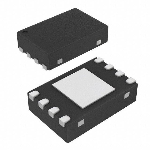
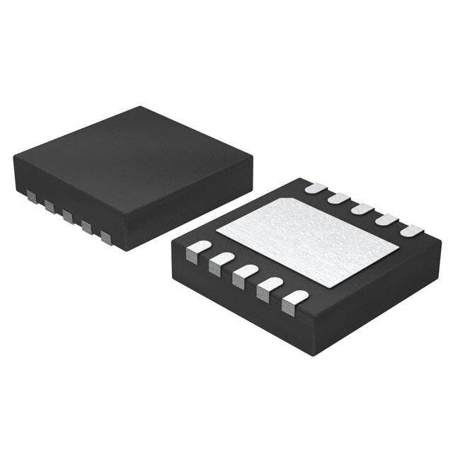
| 产品图片 |
|
| 产品型号 | MAX16809ATU+ |
| rohs | 无铅 / 符合限制有害物质指令(RoHS)规范要求 |
| 产品系列 | - |
| 产品培训模块 | http://www.digikey.cn/PTM/IndividualPTM.page?site=cn&lang=zhs&ptm=25703http://www.digikey.cn/PTM/IndividualPTM.page?site=cn&lang=zhs&ptm=25705 |
| 供应商器件封装 | 38-TQFN(5x7) |
| 内部驱动器 | 是 |
| 包装 | 管件 |
| 安装类型 | 表面贴装 |
| 封装/外壳 | 38-WFQFN 裸露焊盘 |
| 工作温度 | -40°C ~ 125°C |
| 恒压 | - |
| 恒流 | 是 |
| 拓扑 | 开路漏极,PWM,降压(降压),SEPIC,升压(升压) |
| 标准包装 | 43 |
| 电压-电源 | 8 V ~ 26.5 V |
| 电压-输出 | 36V |
| 类型-初级 | 背光 |
| 类型-次级 | RGB,白色 LED |
| 输出数 | 16 |
| 频率 | 20kHz ~ 1MHz |


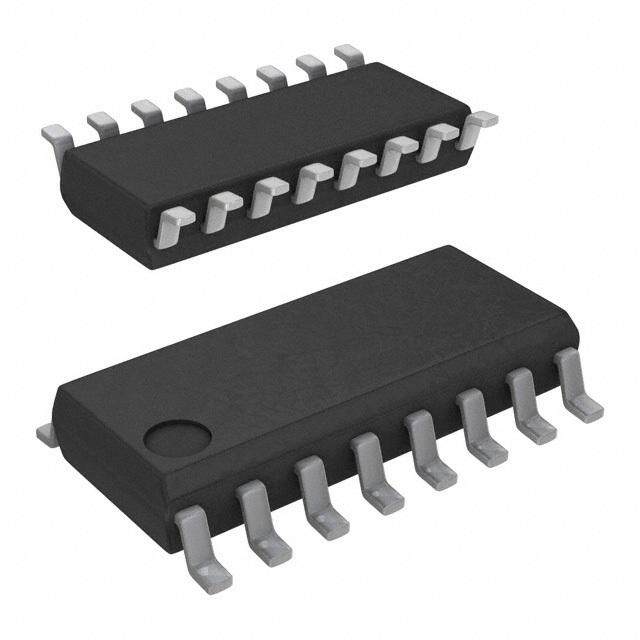


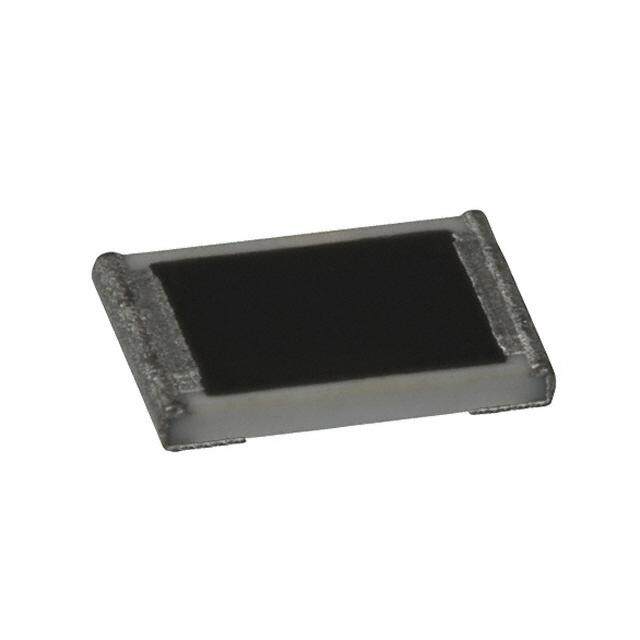

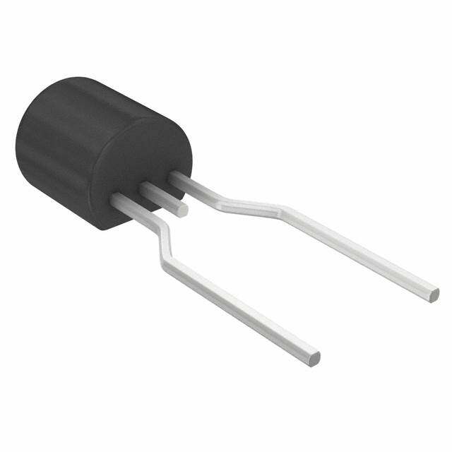

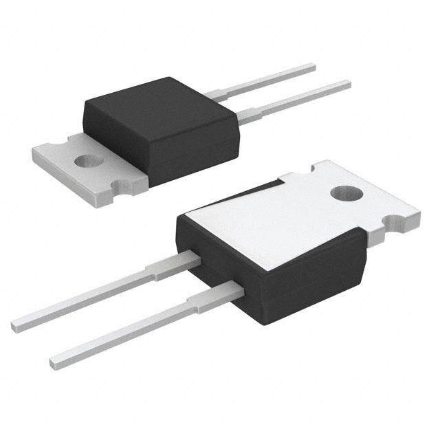
- 商务部:美国ITC正式对集成电路等产品启动337调查
- 曝三星4nm工艺存在良率问题 高通将骁龙8 Gen1或转产台积电
- 太阳诱电将投资9.5亿元在常州建新厂生产MLCC 预计2023年完工
- 英特尔发布欧洲新工厂建设计划 深化IDM 2.0 战略
- 台积电先进制程称霸业界 有大客户加持明年业绩稳了
- 达到5530亿美元!SIA预计今年全球半导体销售额将创下新高
- 英特尔拟将自动驾驶子公司Mobileye上市 估值或超500亿美元
- 三星加码芯片和SET,合并消费电子和移动部门,撤换高东真等 CEO
- 三星电子宣布重大人事变动 还合并消费电子和移动部门
- 海关总署:前11个月进口集成电路产品价值2.52万亿元 增长14.8%


PDF Datasheet 数据手册内容提取
EVALUATION KIT AVAILABLE MAX16809 Integrated 16-Channel LED Driver with Switch-Mode Boost and SEPIC Controller General Description Features The MAX16809 is an integrated, high-efficiency white ● 16 Constant-Current Output Channels (Up to 55mA or RGB LED driver. It is designed for LCD backlighting Each) and other LED lighting applications with multiple strings ● ±3% Current Matching Among Outputs of LEDs. The MAX16809’s current-mode PWM control- ● Paralleling Channels Allows Higher Current per LED ler regulates the necessary voltage to the LED array. String Depending on the input voltage and LED voltage range, ● Outputs Rated for 36V Continuous Voltage this device can be used with boost or buck-boost (SEPIC) ● Output-Enable Pin for PWM Dimming (Up to 30kHz) topologies. ● One Resistor Sets LED Current for All Channels The MAX16809 LED driver includes 16 open-drain, constant-current-sinking LED driver outputs rated for ● Wide Dimming Ratio Up to 5000:1 36V continuous operation. The LED current-control cir- ● Low Current-Sense Reference (300mV) for High cuitry achieves ±3% current matching among strings Efficiency and enables paralleling of outputs for LED string cur- ● 8V to 26.5V Input Voltage or Higher with External rents higher than 55mA. The output-enable pin is used Biasing Devices for simultaneous PWM dimming of all output channels. ● 4-Wire Serial Interface to Control Individual Output Dimming frequency range is 50Hz to 30kHz and dimming Channels ratio is up to 5000:1. The constant-current outputs are single resistor programmable and the LED current can be Applications adjusted up to 55mA per output channel. ● LCD White or RGB LED Backlighting: LCD TVs, Desktop, and Notebook Panels The MAX16809 operates either in stand-alone mode or with a microcontroller (µC) using an industry-standard, Industrial and Medical Displays 4-wire serial interface. ● Ambient, Mood, and Accent Lighting The MAX16809 includes overtemperature protection, operates over the full -40°C to +125°C temperature range, and is available in a 5mm x 7mm thermally enhanced, Ordering Information 38-pin TQFN exposed pad package. PART TEMP RANGE PIN-PACKAGE MAX16809ATU+ -40°C to +125°C 38 TQFN-EP* Pin Configuration appears at end of data sheet. +Denotes a lead(Pb)-free/RoHS-compliant package. *EP = Exposed pad. Typical Operating Circuits VIN L VOUT Q1 COUT R1 LEDs RCS CC2 CC1 RC1 R2 OUTCSAGND COMP 3V TO 5.5V CIN VCC FB V+ OUT0 CBYP PGND OOUUTT12 OUT3 LDODCEIOLENKUT MAX16809 OOOOOOUUUUUUTTTTTT456789 SET OUT10 OUT11 OUT12 OUT13 RSET OOUUTT1145 REF RTCT STAND-ALONE OPERATION RT CREF CT Typical Operating Circuits continued at end of data sheet. 19-0656; Rev 3; 4/14
MAX16809 Integrated 16-Channel LED Driver with Switch-Mode Boost and SEPIC Controller Absolute Maximum Ratings VCC to AGND ........................................................-0.3V to +30V OUT0–OUT15 Sink Current ...............................................60mA Current into VCC (VCC > 24V) ...........................................30mA Total PGND Current (1s pulse time) ................................960mA V+ to PGND ............................................................-0.3V to +6V Continuous Power Dissipation (TA = +70°C) OUT to AGND ...........................................-0.3V to (VCC + 0.3V) 38-Pin TQFN (derate 35.7mW/°C* above +70°C) .....2857mW OUT Current (10µs duration) ................................................±1A Operating Temperature Range .........................-40°C to +125°C FB, COMP, CS, RTCT, REF to AGND ....................-0.3V to +6V Junction Temperature ......................................................+150°C COMP Sink Current ............................................................10mA Storage Temperature Range ............................-65°C to +150°C OUT0–OUT15 to PGND ........................................-0.3V to +40V Lead Temperature (soldering, 10s) .................................+300°C DIN, CLK, LE, OE, SET to PGND ...............-0.3V to (V+ + 0.3V) *Per JEDEC51 Standard (Multilayer Board). DOUT Current ..................................................................±10mA Stresses beyond those listed under “bsolute Maximum Ratings” may cause permanent damage to the device. These are stress ratings only, and functional operation of the device at these or any other conditions beyond those indicated in the operational sections of the specifications is not implied. Exposure to absolute maximum rating conditions for extended periods may affect device reliability. Electrical Characteristics (PWM Controller) (VCC = +15V, V+ = +3V to +5.5V referenced to PGND, RT = 10kΩ, CT = 3.3nF, REF = open, COMP = open, CREF = 0.1µF, VFB = 2V, CS = AGND, AGND = PGND = 0V; all voltages are measured with respect to AGND, unless otherwise noted. TJ = TA = -40°C to +125°C, unless otherwise noted. Typical values are at TA = +25°C.) (Note 1) PARAMETER SYMBOL CONDITIONS MIN TYP MAX UNITS REFERENCE Output Voltage VREF IREF = 1mA, TJ = +25°C 4.95 5 5.05 V Line Regulation ∆VLINE 12V< VCC < 25V, IREF = 1mA 0.4 4 mV Load Regulation ∆VLOAD 1mA < IREF < 20mA 6 50 mV Total Output-Voltage Variation VREFT (Note 2) 4.875 5.125 V Output Noise Voltage VNOISE 10Hz < f < 10kHz 50 µV Output Short-Circuit Current ISHORT VREF = 0V 30 180 mA OSCILLATOR Initial Accuracy TJ = +25°C 51 54 57 kHz Voltage Stability 12V < VCC < 25V 0.2 0.5 % Temperature Stability 1 % RTCT Ramp Peak-to-Peak 1.7 V RTCT Ramp Valley 1.1 V VRTCT = 2V, TJ = +25°C 7.9 8.3 8.7 Discharge Current IDIS mA VRTCT = 2V, -40oC ≤ TJ ≤ +125°C 7.5 8.3 9.0 Frequency Range fOSC 20 1000 kHz ERROR AMPLIFIER FB Input Voltage VFB FB shorted to COMP 2.45 2.5 2.55 V Input Bias Current IB(FB) -0.01 -0.1 µA Open-Loop Gain AVOL 2V ≤ VCOMP ≤ 4V 100 dB Unity-Gain Bandwidth fGBW 1 MHz Power-Supply Rejection Ratio PSRR 12V ≤ VCC ≤ 25V 60 80 dB COMP Sink Current ISINK VFB = 2.7V, VCOMP = 1.1V 2 6 mA COMP Source Current ISOURCE VFB = 2.3V, VCOMP = 5V 0.5 1.2 1.8 mA COMP Output-Voltage High VOH VFB = 2.3V, RCOMP = 15kΩ to AGND 5 5.8 V COMP Output-Voltage Low VOL VFB = 2.7V, RCOMP = 15kΩ to VREF 0.1 1.1 V www.maximintegrated.com Maxim Integrated │ 2
MAX16809 Integrated 16-Channel LED Driver with Switch-Mode Boost and SEPIC Controller Electrical Characteristics (PWM Controller) (continued) (VCC = +15V, V+ = +3V to +5.5V referenced to PGND, RT = 10kΩ, CT = 3.3nF, REF = open, COMP = open, CREF = 0.1µF, VFB = 2V, CS = AGND, AGND = PGND = 0V; all voltages are measured with respect to AGND, unless otherwise noted. TJ = TA = -40°C to +125°C, unless otherwise noted. Typical values are at TA = +25°C.) (Note 1) PARAMETER SYMBOL CONDITIONS MIN TYP MAX UNITS CURRENT-SENSE AMPLIFIER Current-Sense Gain ACS (Notes 3, 4) 2.85 3 3.40 V/V Maximum Current-Sense Signal VCS_MAX (Note 3) 0.275 0.300 0.325 V Power-Supply Rejection Ratio PSRR 12V ≤ VCC ≤ 25V 70 dB Current-Sense Input Bias Current ICS VCOMP = 0V -1 -2.5 µA Current Sense to OUT Delay tPWM 50mV overdrive 60 ns MOSFET DRIVER TJ = -40°C to +85°C (Note 2) 4.5 10 OUT Low-Side On-Resistance VRDS_ONL ISINK = 200mA Ω TJ = -40°C to +125°C 4.5 12 OUT High-Side On-Resistance VRDS_ONH I1S0O0UmRACE = TTJJ == --4400°°CC ttoo ++8152°5C°C (Note 2) 33..55 71.05 Ω Source Current (Peak) ISOURCE CLOAD = 10nF 2 A Sink Current (Peak) ISINK CLOAD = 10nF 1 A Rise Time tR CLOAD = 1nF 15 ns Fall Time tF CLOAD = 1nF 22 ns UNDERVOLTAGE LOCKOUT/STARTUP Startup Voltage Threshold VCC_START 7.98 8.4 8.82 V Minimum Operating Voltage After Turn-On VCC_MIN 7.1 7.6 8.0 V Undervoltage-Lockout Hysteresis UVLOHYST 0.8 V PULSE-WIDTH MODULATION (PWM) Maximum Duty Cycle DMAX 94.5 96 97.5 % Minimum Duty Cycle DMIN 0 % SUPPLY CURRENT Startup Supply Current ISTART VCC = 7.5V 32 65 µA Operating Supply Current ICC VFB = VCS = 0V 3 5 mA VCC Zener Voltage VZ ICC = 25mA 24 26.5 V www.maximintegrated.com Maxim Integrated │ 3
MAX16809 Integrated 16-Channel LED Driver with Switch-Mode Boost and SEPIC Controller Electrical Characteristics (LED Driver) (V+ = +3V to +5.5V, AGND = PGND = 0V; all voltages are measured with respect to PGND, unless otherwise noted. TA = TJ = -40°C to +125°C, unless otherwise noted. Typical values are at TA = +25°C.) (Note 1) PARAMETER SYMBOL CONDITIONS MIN TYP MAX UNITS Operating Supply Voltage V+ 3.0 5.5 V Output Voltage VOUT_ _ 36 V Standby Current (Interface Idle, All RSET = 360Ω, DIN, LE, CLK = PGND or V+, 3.6 4.5 mA Output Ports High Impedance) OE = V+, DOUT unconnected Standby Current (Interface Active, All Output Ports RSET = 360Ω, fCLK = 5MHz, OE = V+, 3.8 4.8 mA DIN, LE = PGND or V+, DOUT unconnected High Impedance) Supply Current (Interface Idle, All Output Ports I+ RSET = 360Ω, OE = PGND, DIN, 30 52.5 mA LE = V+, DOUT unconnected Active Low) INTERFACE (DIN, CLK, DOUT, LE, OE) Input-Voltage High 0.7 (DIN, CLK, LE, OE) VIH x V+ V Input-Voltage Low 0.3 (DIN, CLK, LE, OE) VIL x V+ V Hysteresis Voltage (DIN, CLK, LE, OE) VHYST 0.8 V Input Leakage Current (DIN, CLK) ILEAK -1 +1 µA OE Pullup Current to V+ IOE V+ = 5.5V, OE = PGND 0.25 1.5 25 µA LE Pulldown Current to PGND ILE V+ = 5.5V, LE = V+ 0.25 1.5 25 µA V+ Output-Voltage High (DOUT) VOH ISOURCE = 4mA - 0.5V V Output-Voltage Low (DOUT) VOL ISINK = 4mA 0.5 V 0°C ≤ TA ≤ +125°C, VOUT = 1V to 2.5V, 43.25 47.5 51.75 RSET = 360Ω OUT_ _ Output Current IOUT_ _ mA TA = -40°C, VOUT = 1V to 2.5V, 40 55 RSET = 360Ω OUT_ _ Leakage Current OE = V+ 1 µA www.maximintegrated.com Maxim Integrated │ 4
MAX16809 Integrated 16-Channel LED Driver with Switch-Mode Boost and SEPIC Controller 5V Timing Characteristics (V+ = +4.5V to +5.5V, AGND = PGND = 0V; all voltages are measured with respect to PGND, unless otherwise noted. TA = TJ = -40°C to +125°C, unless otherwise noted. Typical values are at TA = +25°C.) (Notes 1, 5) PARAMETER SYMBOL CONDITION MIN TYP MAX UNITS INTERFACE TIMING CHARACTERISTICS CLK Clock Period tCP 40 ns CLK Pulse-Width High tCH 19 ns CLK Pulse-Width Low tCL 19 ns DIN Setup Time tDS 4 ns DIN Hold Time tDH 8 ns DOUT Propagation Delay tDO 10 50 ns DOUT Rise Time tDR CDOUT = 10pF, 20% to 80% 10 ns DOUT Fall Time tDF CDOUT = 10pF, 80% to 20% 10 ns LE Pulse-Width High tLW 20 ns LE Setup Time tLS 15 ns LE Rising to OUT_ _ Rising Delay tLRR (Note 6) 110 ns LE Rising to OUT_ _ Falling Delay tLRF (Note 6) 340 ns CLK Rising to OUT_ _ Rising Delay tCRR (Note 6) 110 ns CLK Rising to OUT_ _ Falling Delay tCRF (Note 6) 340 ns OE Rising to OUT_ _ Rising Delay tOER (Note 6) 110 ns OE Falling to OUT_ _ Falling Delay tOEF (Note 6) 340 ns OUT_ _ Turn-On Fall Time tF 80% to 20% (Note 6) 210 ns OUT_ _ Turn-Off Rise Time tR 20% to 80% (Note 6) 130 ns www.maximintegrated.com Maxim Integrated │ 5
MAX16809 Integrated 16-Channel LED Driver with Switch-Mode Boost and SEPIC Controller 3.3V Timing Characteristics (V+ = +3V to < +4.5V, AGND = PGND = 0V; all voltages are measured with respect to PGND, unless otherwise noted. TA = TJ = -40°C to +125°C, unless otherwise noted. Typical values are at TA = +25°C.) (Notes 1, 5) PARAMETERS SYMBOL CONDITIONS MIN TYP MAX UNITS INTERFACE TIMING CHARACTERISTICS CLK Clock Period tCP 52 ns CLK Pulse-Width High tCH 24 ns CLK Pulse-Width Low tCL 24 ns DIN Setup Time tDS 4 ns DIN Hold Time tDH 8 ns DOUT Propagation Delay tDO 12 70 ns DOUT Rise Time tDR CDOUT = 10pF, 20% to 80% 12 ns DOUT Fall Time tDF CDOUT = 10pF, 80% to 20% 12 ns LE Pulse-Width High tLW 20 ns LE Setup Time tLS 15 ns LE Rising to OUT_ _ Rising Delay tLRR (Note 6) 140 ns LE Rising to OUT_ _ Falling Delay tLRF (Note 6) 400 ns CLK Rising to OUT_ _ Rising Delay tCRR (Note 6) 140 ns CLK Rising to OUT_ _ Falling Delay tCRF (Note 6) 400 ns OE Rising to OUT_ _ Rising Delay tOER (Note 6) 140 ns OE Falling to OUT_ _ Falling Delay tOEF (Note 6) 400 ns OUT_ _ Turn-On Fall Time tF 80% to 20% (Note 6) 275 ns OUT_ _ Turn-Off Rise Time tR 20% to 80% (Note 6) 150 ns Note 1: This device is 100% production tested at TJ = +25°C and +125°C. Limits to -40°C are guaranteed by design. Note 2: Guaranteed by design, not production tested. Note 3: Parameter is measured at trip point of latch with VFB = 0V. Note 4: Gain is defined as A = ∆VCOMP/∆VCS, 0.05V ≤ VCS ≤ 0.25V. Note 5: See Figures 3 and 4. Note 6: A 65Ω pullup resistor is connected from OUT_ _ to 5.5V. Rising refers to VOUT_ _ when current through OUT_ _ is turned off and falling refers to VOUT_ _ when current through OUT_ _ is turned on. www.maximintegrated.com Maxim Integrated │ 6
MAX16809 Integrated 16-Channel LED Driver with Switch-Mode Boost and SEPIC Controller Typical Operating Characteristics (VCC = +15V, V+ = 3V to 5.5V, RT = 10kΩ, CT = 3.3nF, VREF = COMP = open, CREF = 0.1µF, VFB = 2V, CS = AGND = PGND = 0V. Typical values are at TA = +25°C, unless otherwise noted.) OPERATING SUPPLY CURRENT STARTUP CURRENT vs. TEMPERATURE AFTER STARTUP BOOTSTRAP UVLO vs. TEMPERATURE vs. TEMPERATURE (fOSC = fSW = 300kHz) 1890 VCC RISING MAX16809 toc01 3491 VCC = 7.5V MAX16809 toc02 45..91 CT = 560pF MAX16809 toc03 37 4.7 7 VCC FALLING V (V)CC 456 µI (A)CC 3335 I (mA)CC 44..35 31 4.1 3 29 3.9 2 1 HYSTERESIS 27 3.7 0 25 3.5 -40-25-10 5 20 35 50 65 80 95 110125 -40-25-10 5 20 35 50 65 80 95 110125 -40-25-10 5 20 35 50 65 80 95 110125 TEMPERATURE (°C) TEMPERATURE (°C) TEMPERATURE (°C) REFERENCE VOLTAGE REFERENCE VOLTAGE REFERENCE VOLTAGE vs. TEMPERATURE vs. REFERENCE LOAD CURRENT vs. SUPPLY VOLTAGE 555...000468 MAX16809 toc04 55..0005 MAX16809 toc05 445...990990860 IREF = 1mA MAX16809 toc06 4.95 4.994 5.02 V (V)REF54..0908 IREF = 1mA V (V)REF44..8950 V (V)REF44..999920 4.988 4.96 IREF = 20mA 4.80 4.986 4.75 4.94 4.984 4.92 4.70 4.982 4.90 4.65 4.980 -40-25-10 5 20 35 50 65 80 95 110125 0 10 20 30 40 50 60 70 10 12 14 16 18 20 22 24 26 TEMPERATURE (°C) IREF (mA) VCC (V) OSCILLATOR FREQUENCY (fOSC) OSCILLATOR RT/CT DISCHARGE CURRENT vs. TEMPERATURE vs. TEMPERATURE Y (kHz) 555435000 RCTT == 35.6605pkFΩ MAX16809 toc07 NT (mA)888...000204 VRT/CT = 2V MAX16809 toc08 NC 520 RE QUE 510 CUR7.98 RE 500 GE 7.96 R F AR TO 490 CH7.94 A S OSCILL 447800 R/C DITT7.92 460 7.90 450 7.88 -40-25-10 5 20 35 50 65 80 95 110125 -40-25-10 5 20 35 50 65 80 95 110125 TEMPERATURE (°C) TEMPERATURE (°C) www.maximintegrated.com Maxim Integrated │ 7
MAX16809 Integrated 16-Channel LED Driver with Switch-Mode Boost and SEPIC Controller Typical Operating Characteristics (VCC = +15V, V+ = 3V to 5.5V, RT = 10kΩ, CT = 3.3nF, VREF = COMP = open, CREF = 0.1µF, VFB = 2V, CS = AGND = PGND = 0V. Typical values are at TA = +25°C, unless otherwise noted.) CURRENT-SENSE TRIP THRESHOLD TIMING RESISTANCE OUT IMPEDANCE vs. TEMPERATURE vs. TEMPERATURE vs. OSCILLATOR FREQUENCY (RDS_ON PMOS DRIVER) 000...334860 MAX16809 toc09 1000 CT = 1nF MAX16809 toc10 4445....4680 ISOURCE = 100mA MAX16809 toc11 V)0.34 100 CT = 560pF 4.2 THRESHOLD (000...323082 ΩR (k)T 10 CT = C2T2 0=p 1F00pF ΩR ()DS_ON 33334.....24680 CS 0.26 CT = 10nF 3.0 1 CT = 4.7nF 2.8 0.24 2.6 CT = 3.3nF 2.4 0.22 CT = 2.2nF 2.2 0.20 0.1 2.0 -40-25-10 5 20 35 50 65 80 95 110125 10k 100k 1M 10M -40-25-10 5 20 35 50 65 80 95 110125 TEMPERATURE (°C) FREQUENCY (Hz) TEMPERATURE (°C) OUT IMPEDANCE vs. TEMPERATURE PROPAGATION DELAY FROM CURRENT-LIMIT ERROR-AMPLIFIER OPEN-LOOP GAIN (RDS_ON NMOS DRIVER) COMPARATOR TO OUT vs. TEMPERATURE AND PHASE vs. FREQUENCY ΩR ()DS_ON15467980 ISINK = 200mA MAX16809 toc12 PAGATION DELAY (ns)154679800000000 MAX16809 toc13 GAIN (dB)111468024000000 GAIN PHMAASX1E6809 toc14 -----1196410105055 PHASE (DEGREES) 3 O30 R P 20 -140 2 20 1 10 0 -165 0 0 -20 -190 -40-25-10 5 20 35 50 65 80 95 110125 -40-25-10 5 20 35 50 65 80 95 110125 0.01 1 10 100 1k 10k 100k 1M 10M100M TEMPERATURE (°C) TEMPERATURE (°C) FREQUENCY (Hz) COMP VOLTAGE LEVEL TO TURN SUPPLY CURRENT SUPPLY CURRENT vs. SUPPLY VOLTAGE OFF DEVICE vs. TEMPERATURE vs. OSCILLATOR FREQUENCY (INTERFACE IDLE, ALL OUTPUTS OFF, RSET = 720Ω) 222...213 VCC = 15V MAX16809 toc15 667...500 CT = 100pF MAX16809 toc16 A)12..9050 6A = +125°C TA = +85°C MAX16809 toc17 5.5 m T ( V (V)COMP 112...890 I (mA)CC 454...005 TA = +125°C TA = -40°C PLY CURREN1.90 TA = -40°C TA = +25°C P 3.5 U 1.7 S1.85 3.0 1.6 2.5 1.5 2.0 1.80 -40-25-10 5 20 35 50 65 80 95 110125 20 1202203204205206207208209201020 3.0 3.5 4.0 4.5 5.0 5.5 TEMPERATURE (°C) FREQUENCY (kHz) SUPPLY VOLTAGE (V) www.maximintegrated.com Maxim Integrated │ 8
MAX16809 Integrated 16-Channel LED Driver with Switch-Mode Boost and SEPIC Controller Typical Operating Characteristics (VCC = +15V, V+ = 3V to 5.5V, RT = 10kΩ, CT = 3.3nF, VREF = COMP = open, CREF = 0.1µF, VFB = 2V, CS = AGND = PGND = 0V. Typical values are at TA = +25°C, unless otherwise noted.) SUPPLY CURRENT vs. SUPPLY VOLTAGE SUPPLY CURRENT vs. SUPPLY VOLTAGE (INTERFACE IDLE, ALL OUTPUTS OFF, RSET = 360Ω) (INTERFACE IDLE, ALL OUTPUTS ON, RSET = 720Ω) mA)33..6750 TA = +125°C TA = +85°C MAX16809 toc18 mA) 4405 TA = +125°C TA = +85°C MAX16809 toc19 T ( T ( 35 N N E E R R UR3.60 UR 30 C C LY TA = +25°C LY PP PP 25 SU3.55 TA = -40°C SU TA = +25°C 20 TA = -40°C 3.50 15 3.0 3.5 4.0 4.5 5.0 5.5 3.0 3.5 4.0 4.5 5.0 5.5 SUPPLY VOLTAGE (V) SUPPLY VOLTAGE (V) SUPPLY CURRENT vs. SUPPLY VOLTAGE OUT_ _ CURRENT vs. OUT_ _ VOLTAGE (INTERFACE IDLE, ALL OUTPUTS ON, RSET = 360Ω) (RSET = 720, V+ = 3.3V) mA) 4405 TA = +125°C TA = +85°C MAX16809 toc20 mA) 2350 TA = -40°C MAX16809 toc21 SUPPLY CURRENT ( 233505 TA = +25°C OUT_ _ CURRENT ( 112050 TATT AA= ==+ 1++228555°°°CCC 20 5 TA = -40°C 15 0 3.0 3.5 4.0 4.5 5.0 5.5 0 0.5 1.0 1.5 2.0 2.5 3.0 SUPPLY VOLTAGE (V) OUT_ _ VOLTAGE (V) OUT_ _ CURRENT vs. OUT_ _ VOLTAGE OUT_ _ CURRENT vs. OUT_ _ VOLTAGE (RSET = 360Ω, V+ = 3.3V) (RSET = 720Ω, V+ = 5.0V) 5600 TA = -40°C MAX16809 toc22 2350 TA = -40°C MAX16809 toc23 A) A) m m NT ( 40 TA = +25°C NT ( 20 TA = +25°C E E R R UR 30 TA = +85°C UR 15 TA = +85°C C C _ _ UT_ 20 TA = +125°C UT_ 10 TA = +125°C O O 10 5 0 0 0 0.5 1.0 1.5 2.0 2.5 3.0 0 0.5 1.0 1.5 2.0 2.5 3.0 OUT_ _ VOLTAGE (V) OUT_ _ VOLTAGE (V) www.maximintegrated.com Maxim Integrated │ 9
MAX16809 Integrated 16-Channel LED Driver with Switch-Mode Boost and SEPIC Controller Typical Operating Characteristics (VCC = +15V, V+ = 3V to 5.5V, RT = 10kΩ, CT = 3.3nF, VREF = COMP = open, CREF = 0.1µF, VFB = 2V, CS = AGND = PGND = 0V. Typical values are at TA = +25°C, unless otherwise noted.) OUT_ _ CURRENT vs. OUT_ _ VOLTAGE OUT_ _ CURRENT vs. V+ (RSET = 360Ω, V+ = 5.0V) (RSET = 720Ω, VOUT = 2V) mA) 5600 TA = -40°C MAX16809 toc24 mA)2245..50 TA = +85°C MAX16809 toc25 NT ( 40 TA = +25°C NT ( TA = +125°C RE RE UR 30 TA = +85°C UR24.0 C C UT_ _ 20 TA = +125°C UT_ _ TA = +25°C O O23.5 TA = -40°C 10 0 23.0 0 0.5 1.0 1.5 2.0 2.5 3.0 3.0 3.5 4.0 4.5 5.0 5.5 OUT_ _ VOLTAGE (V) SUPPLY VOLTAGE (V) OUT_ _ CURRENT vs. V+ OUT_ _ CURRENT vs. SET RESISTANCE (RSET = 360Ω, VOUT = 2V) (V+ = 5.0V) 49 MAX16809 toc26 4500 MAX16809 toc27 A) A) m m T ( 48 TA = +25°C T ( REN TA = -40°C REN 30 R R U U C C _ _ _ _ 20 UT 47 UT O TA = +85°C O TA = +125°C 10 46 0 3.0 3.5 4.0 4.5 5.0 5.5 0 1 2 3 4 5 SUPPLY VOLTAGE (V) SET RESISTANCE (kΩ) www.maximintegrated.com Maxim Integrated │ 10
MAX16809 Integrated 16-Channel LED Driver with Switch-Mode Boost and SEPIC Controller Pin Description PIN NAME FUNCTION 1, 31, 32, N.C. No Connection. Not internally connected. Leave unconnected. 36, 38 2 FB Error-Amplifier Inverting Input 3 COMP Error-Amplifier Output 4–11 OUT8–OUT15 LED Driver Outputs. OUT8–OUT15 are open-drain, constant-current-sinking outputs rated for 36V. Active-Low, Output Enable Input. Drive OE low to PGND to enable the OUT0–OUT15. Drive OE 12 OE high to disable OUT0–OUT15. Serial-Data Output. Data is clocked out of the 16-bit internal shift register to DOUT on CLK’s 13 DOUT rising edge. 14 SET LED Current Setting. Connect RSET from SET to PGND to set the LED current. 15 V+ LED Driver Positive Supply Voltage. Bypass V+ to PGND with a 0.1µF ceramic capacitor. 16, 17 PGND Power Ground 18 DIN Serial-Data Input. Data is loaded into the internal 16-bit shift register on CLK’s rising edge. 19 CLK Serial-Clock Input Latch-Enable Input. Data is loaded transparently from the internal shift register(s) to the output 20 LE latch(es) while LE is high. Data is latched into the output latch(es) on LE’s falling edge, and retained while LE is low. 21–28 OUT0–OUT7 LED Driver Outputs. OUT0–OUT7 are open-drain, constant-current-sinking outputs rated for 36V. 29 RTCT PWM Controller Timing Resistor/Capacitor Connection. A resistor RT from RTCT to REF and a capacitor CT from RTCT to AGND set the oscillator frequency. 30 CS PWM Controller Current-Sense Input 33 AGND Analog Ground 34 OUT MOSFET Driver Output OUT. Connects to the gate of the external n-channel MOSFET. 35 VCC Pofo aw e0r.1-SµuFp apnlyd Ian phuigt.h Beyr pvaasluse V cCeCra tmo iAc GcaNpDa cwitiothr .a 0.1µF ceramic capacitor or a parallel combination 37 REF 5V Reference Output. Bypass REF to AGND with a 0.1µF ceramic capacitor. Exposed Paddle. Connect to the ground plane for improved power dissipation. Do not use as the — EP only ground connection. Detailed Description current-sensing feedback circuitry (not simple current mirrors) to ensure very small current variations over The MAX16809 LED driver includes an internal switch- the full allowed range of output voltage (see the Typical mode controller that can be used as a boost or buck-boost Operating Characteristics). The 4-wire serial interface (SEPIC) converter to generate the voltage necessary to comprises a 16-bit shift register and a 16-bit transpar- drive the multiple strings of LEDs. This device incorpo- ent latch. The shift register is written through a clock rates an integrated low-side driver, a programmable oscil- input, CLK, and a data input, DIN, and the data propa- lator (20kHz to 1MHz), an error amplifier, a low-voltage gates to a data output, DOUT. The data output allows (300mV) current sense for higher efficiency, and a 5V multiple drivers to be cascaded and operated together. reference to power up external circuitry (see Figures 1a The contents of the 16-bit shift register are loaded into and 1b). the transparent latch through a latch-enable input, LE. The MAX16809 LED driver includes a 4-wire serial The latch is transparent to the shift register outputs interface and a current-mode PWM controller to gen- when high and latches the current state on the falling erate the necessary voltage for driving 16 open-drain, edge of LE. Each driveoutput is an open-drain, con - constant-current-sinking output ports. The driver uses stant-current sink that should be connected to the www.maximintegrated.com Maxim Integrated │ 11
MAX16809 Integrated 16-Channel LED Driver with Switch-Mode Boost and SEPIC Controller cathode of a string of LEDs connected in series. The The number of channels can be expanded by using the constant-current capability is up to 55mA per output, MAX6970 and MAX6971 family in conjunction with the set for all 16 outputs by an external resistor, RSET. The MAX16809. device can operate in a stand-alone mode (see the Typical Operating Circuits). UVLO VOLTAGE- DIVIDER REFE2.R5EVNCE PRE5RVEG VCC 26.5V THERMAL SHUTDOWN MAX16809 EN_REFVDD BG 5V REG REF SNS REG_OK DELAY VOLTAGE DIVIDER AGND VCC 300mV ILIM S Q OUT R CS CPWM 2R VEA CLK FB COMP R OSC Q RTCT CLK SERIAL-TO-PARALLEL SHIFT REGISTER DIN D0 D1 D2 D3 D4 D5 D6 D7 D8 D9 D10 D11 D12 D13 D14 D15 DOUT OUTPUT LATCHES POWER-ON LE D0 D1 D2 D3 D4 D5 D6 D7 D8 D9 D10 D11 D12 D13 D14 D15 RESET V+ OE V+ CONSTANT-CURRENT SINK STHHUETRDMOAWLN D0 D1 D2 D3 D4 D5 D6 D7 D8 D9 D10 D11 D12 D13 D14 D15 RCEUFERRREENNCTE SET PGND OUT0 OUT1 OUT2 OUT3 OUT4 OUT5 OUT6 OUT7 OUT8 OUT9 OUT10 OUT11 OUT12 OUT13 OUT14 OUT15 Figure 1a. Internal Block Diagram www.maximintegrated.com Maxim Integrated │ 12
MAX16809 Integrated 16-Channel LED Driver with Switch-Mode Boost and SEPIC Controller typically 4.5Ω. The driver can source 2A and sink 1A typi- V+ cally. This allows for the MAX16809 to quickly turn on and off high gate-charge MOSFETs. Bypass VCC with one or more 0.1µF ceramic capacitors to AGND, placed close to MAX16809 68W/L W/L VCC. The average current sourced to drive the external OUT_ _ MOSFET depends on the total gate charge (QG) and 1.23 1.23V REST operating frequency of the converter. The power dissipa- tion in the MAX16809 is a function of the average output 945R drive current (IDRIVE). Use the following equation to cal- culate the power dissipation in the device due to IDRIVE: R IDRIVE = (QG x fSW) PD = (IDRIVE + ICC) x VCC SET PGND where ICC is the operating supply current. See the Typical Operating Characteristics for the operating supply Figure 1b. OUT_ _ Driver Internal Diagram current at a given frequency. Switch-Mode Controller Error Amplifier The MAX16809 includes an internal error amplifier. The Current-Mode Control Loop inverting input is at FB and the noninverting input is The advantages of current-mode control over volt- internally connected to a 2.5V reference. Set the output age-mode control are twofold. First, there is the feed-for- voltage using a resistive divider between output of the ward characteristic brought on by the controller's ability to adjust for variations in the input voltage on a cycle-by- converter VOUT, FB, and AGND. Use the following for- mula to set the output voltage: cycle basis. Second, the stability requirements of the cur- rent-mode controller are reduced to that of a single-pole R1 system unlike the double pole in the voltage-mode control VOUT = 1 + x VFB R2 scheme. The MAX16809 uses a current-mode control loop where the output of the error amplifier is compared to where VFB = 2.5V. the current-sense voltage (VCS). When the current-sense signal is lower than the inverting input of the CPWM com- Oscillator parator, the output of the comparator is low and the switch The oscillator frequency is programmable using an exter- is turned on at each clock pulse. When the current-sense nal capacitor and a resistor at RTCT (see RT and CT signal is higher than the inverting input of the CPWM in the Typical Operating Circuits). RT is connected from comparator, the output is high and the switch is turned off. RTCT to the 5V reference (REF), and CT is connected Undervoltage Lockout (UVLO) from RTCT to AGND. REF charges CT through RT until its voltage reaches 2.8V. CT then discharges through an The turn-on supply voltage for the MAX16809 is 8.4V 8.3mA internal current sink until CT's voltage reaches (typ). Once VCC reaches 8.4V, the reference powers up. 1.1V, at which time CT is allowed to charge through RT There is a 0.8V of hysteresis from the turn-on voltage again. The oscillator's period is the sum of the charge to the UVLO threshold. Once VCC reaches 8.4V, the and discharge times of CT. Calculate the charge time as MAX16809 operates with VCC down to 7.6V. Once VCC follows: goes below 7.6V (typ), the device is in UVLO. When in UVLO, the quiescent supply current into VCC falls back to tC = 0.57 x RT x CT 32µA (typ), and OUT and REF are pulled low. where tC is in seconds, RT in ohms (Ω), and CT in Farads (F). MOSFET Driver The discharge time is then: OUT drives an external n-channel MOSFET and swings from AGND to VCC. Ensure that VCC remains below the tD = (RT x CT x 1000) / [(4.88 x RT) - (1.8 x 1000)] absolute maximum VGS rating of the external MOSFET. where tD is in seconds, RT in ohms (Ω), and CT in OUT is a push-pull output with the on-resistance of the Farads (F). pMOS typically 3.5Ω and the on-resistance of the nMOS www.maximintegrated.com Maxim Integrated │ 13
MAX16809 Integrated 16-Channel LED Driver with Switch-Mode Boost and SEPIC Controller The oscillator frequency is then: RCS = VCS 1 IP−P fOSC = (tC + tD) IP-P is the peak current that flows through the MOSFET. Reference Output When the voltage produced by this current (through the REF is a 5V reference output that can source 20mA. current-sense resistor) exceeds the current-limit com- Bypass REF to AGND with a 0.1µF capacitor. parator threshold, the MOSFET driver (OUT) turns the switch off within 60ns. In most cases, a small RC filter is Current Limit required to filter out the leading-edge spike on the sense The MAX16809 includes a fast current-limit comparator waveform. Set the time constant of the RC filter at 50ns. to terminate the ON cycle during an overload or a fault condition. The current-sense resistor, RCS, connected Buck-Boost (SEPIC) Operation between the source of the external MOSFET and Figure 2 shows a buck-boost application circuit using AGND, sets the current limit. The CS input has a volt- the MAX16809 in a stand-alone mode of operation. age trip level (VCS) of 0.3V. Use the following equation SEPIC topology is necessary when the total forward to calculate RCS: voltage of the LEDs in a string is such that VOUT can be below or above VIN. VIN L1 C1 D VOUT COUT Q1 L2 R1 RCS CC2 CC1 RC1 R2 OUT CSAGND COMP VCC FB CIN 3V TO 5.5V V+ OUT0 CBYP OUT1 PGND OUT2 OUT3 MAX16809 OUT4 DIN OUT5 LE OUT6 OUT7 EXTERNAL CLK OUT8 CLOCK INPUT DOUT OUT9 EXTERNAL OE OUT10 DIM INPUT OUT11 OUT12 OUT13 OUT14 SET OUT15 REF RTCT RT RSET CREF CT Figure 2. Buck-Boost (SEPIC) Operation www.maximintegrated.com Maxim Integrated │ 14
MAX16809 Integrated 16-Channel LED Driver with Switch-Mode Boost and SEPIC Controller LED Driver LE is the latch-enable input of the MAX16809 that trans- fers data from the 16-bit shift register to its 16-bit output 4-Wire Interface latches (transparent latch). The data latches on the The MAX16809 also operates in a stand-alone mode (see falling edge of LE (Figure 4). The fourth input (OE) pro- the Typical Operating Circuits). For use with a microcon- vides output-enable control of the output drivers. When troller, the MAX16809 features a 4-wire serial interface OE is driven high, the outputs (OUT0–OUT15) are forced using DIN, CLK, LE, OE inputs and DOUT as a data to high impedance without altering the contents of the output. This interface is used to write the LED channels? output latches. Driving OE low enables the outputs to fol- data to the MAX16809. The serial-interface data word low the state of the output latches. OE is independent of length is 16 bits, D0?D15. See Figure 3. the serial interface operation. Data can be shifted into The functions of the five interface pins are as follows: the serial-interface shift register and latched, regardless of the state of OE. DOUT is the serial-data output that DIN is the serial-data input, and must be stable when it shifts data out from the MAX16809's 16-bit shift regis- is sampled on the rising edge of CLK. Data is shifted in ter on the rising edge of CLK. Data at DIN propagates MSB first. This means that data bit D15 is clocked in first, through the shift register and appears at DOUT 16 clock followed by 15 more data bits, finishing with the LSB, D0. cycles later. Table 1 shows the 4-wire serial-interface truth CLK is the serial-clock input that shifts data at DIN into the table. MAX16809's 16-bit shift register on its rising edge. Table 1. 4-Wire Serial-Interface Truth Table SERIAL CLOCK LOAD BLANKING OUTPUT CONTENTS DATA SHIFT REGISTER CONTENTS LATCH CONTENTS INPUT INPUT INPUT CURRENT AT OUT_ _ INPUT DIN CLK D0 D1 D2 … Dn-1 Dn LE D0 D1 D2 … Dn-1 Dn OE D0 D1 D2 … Dn-1 Dn H H R0 R1 … Rn-2 Rn-1 L L R0 R1 … Rn-2 Rn-1 X R0 R1 R2 … Rn-1 Rn X X X … X X L R0 R1 R2 … Rn-1 Rn P0 P1 P2 … Pn-1 Pn H P0 P1 P2 … Pn-1 Pn L P0 P1 P2 … Pn-1 Pn X X X … X X H L L L … L L L = Low Logic Level H = High Logic Level X = Don't Care P = Present State (Shift Register) R = Previous State (Latched) www.maximintegrated.com Maxim Integrated │ 15
MAX16809 Integrated 16-Channel LED Driver with Switch-Mode Boost and SEPIC Controller LE tLW tCL tCH tLS tCP CLK tDH tDS DIN D15 D14 D1 D0 tDO DOUT D15 tOEW OE tOEF tOER 80% OUT_ _ 20% tF tR Figure 3. 4-Wire Serial-Interface Timing Diagram Selecting External Component LE RSET to Set LED Output Current tLRF OUT_ _ The MAX16809 uses an external resistor, RSET, to set the LED current for outputs OUT0–OUT15. The minimum allowed value of RSET is 311Ω, which sets the output currents to 55mA. The maximum allowed value of RSET is LE tLRR 5kΩ (IOUT_ _ = 3.6mA) and the maximum allowed capac- itance at SET is 100pF. OUT_ _ Use the following formula to set the output current: CLK 17,100V tCRF RSET = OUT_ _ IOUT_ _ where IOUT_ _ is the desired output current in milliamps CLK tCRR and the value for RSET is in ohms. OUT_ _ Overtemperature Cutoff The MAX16809 contains an internal temperature sen- Figure 4. LE and CLK to OUT_ _ Timing sor that turns off all outputs when the die temperature exceeds +165°C. The outputs are enabled again when the die temperature drops below +140°C. Register con- tents are not affected, so when a driver is overdissipating, the external symptom is the load LEDs cycling on and off as the driver repeatedly overheats and cools, alternately turning itself off and then back on again. www.maximintegrated.com Maxim Integrated │ 16
MAX16809 Integrated 16-Channel LED Driver with Switch-Mode Boost and SEPIC Controller Stand-Alone Operation where: In stand-alone operation, the MAX16809 does not use V+ = supply voltage the 4-wire interface (see the Typical Operating Circuits). I+ = V+ operating supply current Connect DIN and LE to V+ and provide at least 16 DUTY = PWM duty cycle applied to OE external clock pulses to CLK to enable 16 output ports. This startup pulse sequence can be provided either using VOUTi = MAX16809 port output voltage when driving load an external clock or the PWM signal. The external clock LED(s) can also be generated using the signal at RTCT and an IOUTi = LED drive current programmed by RSET external comparator. PD = power dissipation LED Dimming PCB Layout Guidelines PWM Dimming Careful PCB layout is critical to achieve low switching All the output channels can be dimmed simultaneously losses and clean, stable operation. Use a multilayer board by applying a PWM signal (50Hz to 30kHz) to OE. This whenever possible for better noise immunity. Protect allows for a wide range of dimming up to a 5000:1 ratio. sensitive analog grounds by using a star ground con- Each channel can be independently turned on and off figuration. Minimize ground noise by connecting AGND, using a 4-wire serial interface. The dimming is proportion- PGND, the input bypass-capacitor ground lead, and the al to the PWM duty cycle. output-filter ground lead to a single point (star ground con- figuration). Also, minimize trace lengths to reduce stray LED Current Amplitude Adjustment capacitance, trace resistance, and radiated noise. The Using an analog or digital potentiometer as RSET allows trace between the output voltage-divider and the FB pin for LED current amplitude adjustment and linear dimming. must be kept short, as well as the trace between AGND and PGND. Computing Power Dissipation Use the following equation to estimate the upper limit power dissipation (PD) for the MAX19: i = 15 PD = DUTY× (V+x I +) + ∑ VOUTi x IOUTi i = 0 + (VCC x ICC) www.maximintegrated.com Maxim Integrated │ 17
MAX16809 Integrated 16-Channel LED Driver with Switch-Mode Boost and SEPIC Controller Typical Operating Circuits (continued) VIN VOUT L D LEDs COUT R1 CC2 RCS CC1 RC1 R2 OUT CSAGND COMP VCC FB CIN 3V TO 5.5V V+ OUT0 CBYP OUT1 PGND OUT2 OUT3 OUT4 MAX16809 OUT5 OUT6 OUT7 SCLK CLK OUT8 MOSI DIN OUT9 µC MISO DOUT OUT10 LOAD LE OUT11 ENABLE OE OUT12 OUT13 OUT14 SET OUT15 REF RTCT OPERATION WITH MICROCONTROLLER RT RSET CREF CT www.maximintegrated.com Maxim Integrated │ 18
MAX16809 Integrated 16-Channel LED Driver with Switch-Mode Boost and SEPIC Controller Pin Configuration Chip Information PROCESS: BiCMOS TOP VIEW N.C. CS RTCT OUT7 OUT6 OUT5 OUT4 OUT3 OUT2 OUT1 OUT0 LE 31 30 29 28 27 26 25 24 23 22 21 20 N.C. 32 19 CLK Package Information AGND 33 18 DIN For the latest package outline information and land patterns OUT 34 17 PGND (footprints), go to www.maximintegrated.com/packages. Note VCC 35 MAX16809 16 PGND that a “+”, “#”, or “-” in the package code indicates RoHS status N.C. 36 15 V+ only. Package drawings may show a different suffix character, but REF 37 14 SET the drawing pertains to the package regardless of RoHS status. N.C. 38 13 DOUT + PACKAGE PACKAGE OUTLINE LAND 1 2 3 4 5 6 7 8 9 10 11 12 TYPE CODE NO. PATTERN NO. N.C. FB COMP OUT8 OUT9 OUT10 OUT11 OUT12 OUT13 OUT14 OUT15 OE 38 TQFN-EP T3857M+1 21-0172 90-0007 TQFN www.maximintegrated.com Maxim Integrated │ 19
MAX16809 Integrated 16-Channel LED Driver with Switch-Mode Boost and SEPIC Controller Revision History REVISION REVISION PAGES DESCRIPTION NUMBER DATE CHANGED 0 10/06 Initial release — 1 3/07 Released the MAX16810 on the data sheet. 1, 14, 16, 22, 23 2 8/09 Removed the MAX16810 from the data sheet. 1–20 3 4/14 No /V OPNs; removed Automotive reference from Applications section 1 For pricing, delivery, and ordering information, please contact Maxim Direct at 1-888-629-4642, or visit Maxim Integrated’s website at www.maximintegrated.com. Maxim Integrated cannot assume responsibility for use of any circuitry other than circuitry entirely embodied in a Maxim Integrated product. No circuit patent licenses are implied. Maxim Integrated reserves the right to change the circuitry and specifications without notice at any time. The parametric values (min and max limits) shown in the Electrical Characteristics table are guaranteed. Other parametric values quoted in this data sheet are provided for guidance. Maxim Integrated and the Maxim Integrated logo are trademarks of Maxim Integrated Products, Inc. © 2014 Maxim Integrated Products, Inc. │ 20