ICGOO在线商城 > MAX218CWP+

 Datasheet下载
- 型号: MAX218CWP+
- 制造商: Maxim
- 库位|库存: xxxx|xxxx
- 要求:
| 数量阶梯 | 香港交货 | 国内含税 |
| +xxxx | $xxxx | ¥xxxx |
查看当月历史价格
查看今年历史价格
MAX218CWP+产品简介:
ICGOO电子元器件商城为您提供MAX218CWP+由Maxim设计生产,在icgoo商城现货销售,并且可以通过原厂、代理商等渠道进行代购。 提供MAX218CWP+价格参考以及MaximMAX218CWP+封装/规格参数等产品信息。 你可以下载MAX218CWP+参考资料、Datasheet数据手册功能说明书, 资料中有MAX218CWP+详细功能的应用电路图电压和使用方法及教程。
| 参数 | 数值 |
| 产品目录 | 集成电路 (IC)半导体 |
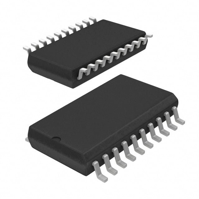
| 描述 | IC TXRX RS232 DL 120KBPS 20SOICRS-232接口集成电路 1.8-4.25V True RS232 Dual Transceiver |
| 产品分类 | |
| 品牌 | Maxim Integrated |
| 产品手册 | |
| 产品图片 |
|
| rohs | 符合RoHS无铅 / 符合限制有害物质指令(RoHS)规范要求 |
| 产品系列 | 接口 IC,RS-232接口集成电路,Maxim Integrated MAX218CWP+- |
| 数据手册 | |
| 产品型号 | MAX218CWP+ |
| 产品培训模块 | http://www.digikey.cn/PTM/IndividualPTM.page?site=cn&lang=zhs&ptm=25703http://www.digikey.cn/PTM/IndividualPTM.page?site=cn&lang=zhs&ptm=25705 |
| 产品目录页面 | |
| 产品种类 | RS-232接口集成电路 |
| 传播延迟时间ns | 2.7 us, 0.7 us |
| 供应商器件封装 | 20-SOIC W |
| 关闭 | Yes |
| 功能 | Transceiver |
| 包装 | 管件 |
| 协议 | RS232 |
| 双工 | 全 |
| 商标 | Maxim Integrated |
| 安装类型 | 表面贴装 |
| 安装风格 | SMD/SMT |
| 封装 | Tube |
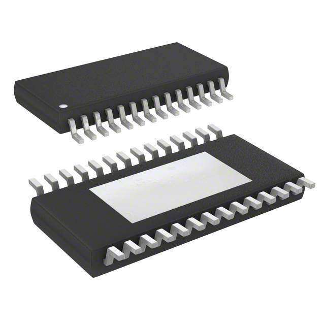
| 封装/外壳 | 20-SOIC(0.295",7.50mm 宽) |
| 封装/箱体 | SO-Wide-20 |
| 工作温度 | 0°C ~ 70°C |
| 工作温度范围 | 0 C to + 70 C |
| 工作电源电压 | 3 V |
| 工厂包装数量 | 36 |
| 应用说明 | |
| 接收器滞后 | 100mV |
| 接收机数量 | 2 Receiver |
| 数据速率 | 120 kb/s |
| 最大工作温度 | + 70 C |
| 最小工作温度 | 0 C |
| 标准包装 | 1 |
| 激励器数量 | 2 Driver |
| 电压-电源 | 1.8 V ~ 4.25 V |
| 电源电流 | 3 mA |
| 类型 | 收发器 |
| 系列 | MAX218C |
| 输入/输出端数量 | 8 |
| 零件号别名 | MAX218C |
| 驱动器/接收器数 | 2/2 |









PDF Datasheet 数据手册内容提取
19-0246; Rev 1; 7/95 1.8V to 4.25V-Powered, True RS-232 Dual Transceiver _______________General Description ____________________________Features M The MAX218 RS-232 transceiver is intended for battery- BETTER THAN BIPOLAR! A powered EIA/TIA-232E and V.28/V.24 communications 'Operates Directly from Two Alkaline, NiCd, X interfaces that need two drivers and two receivers with or NiMH Cells minimum power consumption. It provides a wide +1.8V 2 to +4.25V operating voltage range while maintaining '+1.8V to +4.25V Supply Voltage Range 1 true RS-232 and EIA/TIA-562 voltage levels. The '120kbps Data Rate 8 MAX218 runs from two alkaline, NiCd, or NiMH cells without any form of voltage regulator. 'Low-Cost Surface-Mount Components A shutdown mode reduces current consumption to 'Meets EIA/TIA-232E Specifications 1µA, extending battery life in portable systems. While '1µA Low-Power Shutdown Mode shut down, all receivers can remain active or can be 'Both Receivers Active During Low-Power Shutdown disabled under logic control, permitting a system incor- porating the CMOS MAX218 to monitor external 'Three-State Receiver Outputs devices while in low-power shutdown mode. ' A guaranteed 120kbps data rate provides compatibility 'On-Board DC-DC Converters with popular software for communicating with personal computers. Three-state drivers are provided on all '20-Pin SSOP, Wide SO, or DIP Packages receiver outputs so that multiple receivers, generally of different interface standards, can be wire-ORed at the ______________Ordering Information UART. The MAX218 is available in 20-pin DIP, SO, and SSOP packages. PART TEMP. RANGE PIN-PACKAGE ________________________Applications MAX218CPP 0°C to +70°C 20 Plastic DIP MAX218CWP 0°C to +70°C 20 Wide SO Battery-Powered Equipment MAX218CAP 0°C to +70°C 20 SSOP Computers MAX218C/D 0°C to +70°C Dice* Printers MAX218EPP -40°C to +85°C 20 Plastic DIP Peripherals MAX218EWP -40°C to +85°C 20 Wide SO Instruments MAX218EAP -40°C to +85°C 20 SSOP Modems *Contact factory for dice specifications. __________Typical Operating Circuit __________________Pin Configuration TOP VIEW 1 19 1T.8OV(cid:13)(cid:13) 6 VCC LX V+ V- 15 N.LCX. 12 2109 GV+ND 4.25V MAX218 C1+ 18 SHDN 3 18 C1+ ON/OFF 3 SHDN C1- 16 EN 4 17 GND 7 T1IN T1 T1OUT 14 GND 5 MAX218 16 C1- VCC 6 15 V- 8 T2IN T2 T2OUT 13 T1IN 7 14 T1OUT 9 R1OUT R1IN 12 T2IN 8 13 T2OUT R1OUT 9 12 R1IN 10 R2OUT R2IN 11 R2 R2OUT 10 11 R2IN EN GND ENABLE 4 5, 17, 20 DIP/SO/SSOP ________________________________________________________________Maxim Integrated Products 1 Call toll free 1-800-998-8800 for free samples or literature.
1.8V to 4.25V-Powered, True RS-232 Dual Transceiver 8 ABSOLUTE MAXIMUM RATINGS 1 Supply Voltages Short-Circuit Duration, R_OUT, T_OUT to GND .......Continuous 2 VCC....................................................................-0.3V to +4.6V Continuous Power Dissipation (TA= +70°C) X V+..........................................................(VCC- 0.3V) to +7.5V Plastic DIP (derate 11.11mW/°C above +70°C)..........889mW V-.......................................................................+0.3V to -7.4V Wide SO (derate 10.00mW/°C above +70°C)..............800mW A VCCto V-..........................................................................+12V SSOP (derate 8.00mW/°C above +70°C)...................640mW M LX................................................................-0.3V to (1V + V+) Operating Temperature Ranges Input Voltages MAX218C_ P..................................................... 0°C to +70°C ———– T_IN, EN, SHDN .................................................-0.3V to +7V MAX218E_ P...................................................-40°C to +85°C R_IN.................................................................................±25V Storage Temperature Range ...........................-65°C to +150°C Output Voltages Lead Temperature (soldering, 10sec) ...........................+300°C T_OUT.............................................................................±15V) R_OUT....................................................-0.3V to (VCC+ 0.3V) Stresses beyond those listed under “Absolute Maximum Ratings” may cause permanent damage to the device. These are stress ratings only, and functional operation of the device at these or any other conditions beyond those indicated in the operational sections of the specifications is not implied. Exposure to absolute maximum rating conditions for extended periods may affect device reliability. ELECTRICAL CHARACTERISTICS (Circuit of Figure 1, VCC= 1.8V to 4.25V, C1 = 0.47µF, C2 = C3 = C4 = 1µF, L1 = 15µH, TA= TMINto TMAX, unless otherwise noted. Typical values are at VCC= 3.0V, TA= +25°C.) PARAMETER CONDITIONS MIN TYP MAX UNITS DC CHARACTERISTICS Operating Voltage Range 1.8 4.25 V ———– Supply Current (Note 1) No load, VCC= EN = SHDN= 3.0V, TA= +25°C 1.9 3.0 mA ———– SHDN= EN = 0V, all R_INs static 0.04 10 Shutdown Supply Current ———– µA SHDN= 0V, EN = VCC, all R_INs static 0.04 10 LOGIC ———– Input Logic Threshold Low T_IN, EN, SHDN 0.33 x VCC V ———– Input Logic Threshold High T_IN, EN, SHDN 0.67 x VCC V Input Hysteresis T_IN 0.1 V ———– Input Leakage Current T_IN, EN, SHDN= 0V or VCC 0.001 ±1 µA Output Voltage Low R_OUT, IOUT= 1.0mA 0.4 V Output Voltage High R_OUT, IOUT= -0.4mA VCC- 0.25 VCC- 0.08 V Output Leakage Current R_OUT, 0V ≤R_OUT ≤VCC, EN = 0V 0.05 ±10 µA EIA/TIA-232E RECEIVER INPUTS Input Voltage Range -25 +25 V VCC= 2.0V to 4.25V 0.4 Input Threshold Low V VCC= 1.8V to 4.25V 0.3 VCC= 1.8V to 4.25V 3.0 Input Threshold High V VCC= 1.8V to 3.6V 2.8 Input Hysteresis 0.7 V Input Resistance -15V < R_IN < +15V 3 5 7 kΩ EIA/TIA-232E TRANSMITTER OUTPUTS Output Voltage Swing All transmitter outputs loaded with 3kΩto ground ±5 ±6 V Output Resistance VCC= 0V, -2V < T_OUT < +2V 300 Ω Output Short-Circuit Current ±24 ±100 mA Note 1: Entire supply current for the circuit of Figure 1. 2 _______________________________________________________________________________________
1.8V to 4.25V-Powered, True RS-232 Dual Transceiver TIMING CHARACTERISTICS M (Circuit of Figure 1, VCC= 1.8V to 4.25V, C1 = 0.47µF, C2 = C3 = C4 = 1µF, L1 = 15µH, TA= TMINto TMAX, unless otherwise noted. A Typical values are at VCC= 3.0V, TA= +25°C.) X PARAMETER SYMBOL CONDITIONS MIN TYP MAX UNITS 2 1000pF ||3kΩload each transmitter, Data Rate 120 kbps 1 150pF load each receiver 8 Receiver Output Enable Time tER 90 300 ns Receiver Output Disable Time tDR 200 500 ns Transmitter Output Enable Time tET 140 450 µs Transmitter Output Disable Time tDT 500 ns tPHLR 150pF load 290 700 Receiver Propagation Delay ns tPLHR 150pF load 260 700 tPHLT 2500pF ||3kΩload 1.9 2.7 Transmitter Propagation Delay µs tPLHT 2500pF ||3kΩload 1.8 2.7 TA= +25°C, VCC= 3.0V, RL= 3kΩto 7kΩ, Transition Region Slew Rate CL= 50pF to 2500pF, measured from 3.0 30 V/µs +3V to -3V or -3V to +3V ______________________________________________________________Pin Description PIN NAME FUNCTION 1 LX Inductor/Diode Connection Point 2 N.C. Not internally connected 3 S—H—D—N– Shutdown Control. Connect to VCCfor normal operation. Connect to GND to shut down the power supply and to disable the drivers. Receiver status is not changed by this control. 4 EN Receiver Output Enable Control. Connect to VCCfor normal operation. Connect to GND to force the receiver outputs into high-Z state. 5, 17, 20 GND Ground. Connect all GND pins to ground. Supply Voltage Input; 1.8V to 4.25V. Bypass to GND with at least 1µF. See Capacitor 6 VCC Selectionsection. 7, 8 T1IN, T2IN Transmitter Inputs 9, 10 R1OUT, R2OUT Receiver Outputs; swing between GND and VCC. 11, 12 R2IN, R1IN Receiver Inputs 13, 14 T2OUT, T1OUT Transmitter Outputs; swing between V+ and V-. 15 V- Negative Supply generated on-board 16, 18 C1-, C1+ Terminals for Negative Charge-Pump Capacitor 19 V+ Positive Supply generated on-board _______________________________________________________________________________________ 3
1.8V to 4.25V-Powered, True RS-232 Dual Transceiver 8 __________________________________________Typical Operating Characteristics 1 (Circuit of Figure 1, VCC= 1.8V, all transmitter outputs loaded with 3kΩ, TA = +25°C, unless otherwise noted.) 2 X SUPPLY CURRENT vs.(cid:13) TRANSMITTING SUPPLY CURRENT(cid:13) SUPPLY VOLTAGE vs. LOAD CAPACITANCE A M 112400 11R LTT RR= AA3NNkWSSMM +II TT2TT5EE0RR0p F1FU/8L DL ADTAAT AR ARTAET(cid:13)E(cid:13) MAX3218-01 19000 VCC = 2.4V MAX3218-02 mA) 100 mA) 80 235kbps RENT ( 80 240kbps RENT ( 70 TATRRT AASNNPSSEMMCIIIFTTITTEEEDRR B 12IT OO RPPAEETRREAA,TT (cid:13)IINNGG (cid:13)(cid:13) UR UR 60 AT 1/16 THAT RATE.(cid:13) UPPLY C 6400 20kbp1s20kbps UPPLY C 50 120kbps (cid:13) S S 40 20 0kbps 30 20kbps 0 20 1.8 2.4 3.0 3.6 4.2 0 1000 2000 3000 4000 5000 SUPPLY VOLTAGE (V) LOAD CAPACITANCE (pF) TIME TO EXIT SHUTDOWN(cid:13) (ONE TRANSMITTER HIGH,(cid:13) ONE TRANSMITTER LOW) SHDN VOH 2V/div T_OUT VRCLC = = 3 1k.W 8V|(cid:13)| 2500pF VOL 100m s/div TRANSMITTER OUTPUT VOLTAGE vs. (cid:13) SLEW RATE vs.(cid:13) LOAD CAPACITANCE AT 120kbps TRANSMITTER CAPACITANCE GE (V) 68 VOUT+ MAX3218-04 1102 MAX3218-05 SMITTER OUTPUT VOLTA --02442 mSLEW RATE (V/s) 486 DATA RA-TSEL E1W20k+bSpLs,E(cid:13)W TRAN -6 VOUT- 2 T3RkWAN PSLMUIST TINEDRISC ALOTEADD ECDA PWAICTIHT A(cid:13)NCE(cid:13) (cid:13) -8 0 0 1000 2000 3000 4000 5000 0 1000 2000 3000 4000 5000 LOAD CAPACITANCE (pF) LOAD CAPACITANCE (pF) 4 _______________________________________________________________________________________
1.8V to 4.25V-Powered, True RS-232 Dual Transceiver The transmitters and receivers are guaranteed to oper- M D1(cid:13) ate at 120kbps data rates, providing compatibility with 15m H 1N6050 A LapLink™ and other high-speed communications soft- 1 19 1m F(cid:13) ware. A shutdown mode extends battery life by reduc- X C2 ing supply current to 0.04µA. While shut down, all 1.8V(cid:13) 6 LX V+ 15 receivers can either remain active or be disabled under 2 4.T2O5(cid:13)V 1m F(cid:13) VCC V- 1m F(cid:13) logic control. With this feature, the MAX218 can be in 1 C4 18 C3 low-power shutdown mode and still monitor activity on 8 MAX218 C1+ 0.47m F(cid:13) external devices. Three-state drivers are provided on ON/OFF 3 SHDN C1- 16 C1 both receiver outputs. Switch-Mode Power Supply 7 T1IN T1OUT 14 T1 The switch-mode power supply uses a single inductor with one diode and three small capacitors to generate 8 T2IN T2OUT 13 ±6.5V from an input voltage in the 1.8V to 4.25V T2 range. 9 R1OUT R1IN 12 R1 Inductor Selection Use a 15µH inductor with a saturation current rating of at 10 R2OUT R2IN 11 least 350mA and less than 1Ωresistance. Table 1 lists R2 suppliers of inductors that meet the 15µH/350mA/1Ω EN GND specifications. 4 5, 17, 20 ENABLE Diode Selection Key diode specifications are fast recovery time (<10ns), Figure 1.Single-Supply Operation average current rating (>100mA), and peak current rat- ing (>350mA). Inexpensive fast silicon diodes, such as the 1N6050, are generally recommended. More expen- sive Schottky diodes improve efficiency and give slightly _______________Detailed Description better performance at very low VCC voltages. Table 1 lists suppliers of both surface-mount and through-hole The MAX218 line driver/receiver is intended for battery- diodes. 1N914s are usually satisfactory, but specifica- powered EIA/TIA-232 and V.28/V.24 communications tions and performance vary widely with different manu- interfaces that require two drivers and two receivers. facturers. The operating voltage extends from 1.8V to 4.25V, yet the device maintains true RS-232 and EIA/TIA-562 Capacitor Selection transmitter output voltage levels. This wide supply volt- Use capacitors with values at least as indicated in age range permits direct operation from a variety of Figure 1. Capacitor C2 determines the ripple on V+, batteries without the need for a voltage regulator. For but not the absolute voltage. Capacitors C1 and C3 example, the MAX218 can be run directly from a single determine both the ripple and the absolute voltage of lithium cell or a pair of alkaline cells. It can also be run V-. Bypass VCCto GND with at least 1µF (C4) placed directly from two NiCd or NiMH cells from full-charge close to pins 5 and 6. If the VCCline is not bypassed voltage down to the normal 0.9V/cell end-of-life point. elsewhere (e.g., at the power supply), increase C4 to The 4.25V maximum supply voltage allows the two 4.7µF. rechargeable cells to be trickle- or fast-charged while You may use ceramic or polarized capacitors in all driving the MAX218. locations. If you use polarized capacitors, tantalum The circuit comprises three sections: power supply, types are preferred because of the high operating fre- transmitters, and receivers. The power-supply section quency of the power supplies (about 250kHz). If alu- converts the supplied input voltage to 6.5V, providing the minum electrolytics are used, higher capacitance val- voltages necessary for the drivers to meet true RS-232 ues may be required. levels. External components are small and inexpensive. ™ LapLink is a trademark of Traveling Software, Inc. _______________________________________________________________________________________ 5
1.8V to 4.25V-Powered, True RS-232 Dual Transceiver 8 Table 1. Suggested Component Suppliers 1 2 MANUFACTURER PART NUMBER PHONE FAX X Inductors—Surface Mount A USA (404) 436-1300 USA (404) 436-3030 Murata-Erie LQH4N150K-TA Japan (075) 951-9111 Japan (075) 955-6526 M USA (708) 956-0666 USA (708) 956-0702 Sumida CD43150 Japan (03) 3607-5111 Japan (03) 3607-5428 USA (708) 803-6100 USA (708) 803-6296 TDK NLC453232T-150K Japan (03) 3278-5111 Japan (03) 3278-5358 Diodes—Surface Mount Central Semiconductor CMPSH-3, Schottky USA (516) 435-1110 USA (516) 435-1824 Motorola MMBD6050LT1, Silicon USA (408) 749-0510 USA (408) 991-7420 Philips PMBD6050, Silicon USA (401) 762-3800 USA (401) 767-4493 Diodes—Through-Hole 1N6050, Silicon Motorola USA (408) 749-0510 USA (408) 991-7420 1N5817, Schottky RS-232 Drivers Shutdown ———– The two drivers are identical, and deliver EIA/TIA-232E WhenSHDNis low, the power supplies are disabled and and EIA/TIA-562 output voltage levels when VDD is the transmitters are put into a high-impeda—nc—e— –state. between 1.8V and 4.25V. The transmitters drive up to Receiver operation is not affected by taking SHDNlow. 3kΩin parallel with 1000pF at up to 120kbps. Connect Power consumption is dramatically reduced in shutdown unused driver inp—ut—s —to– either GND or VCC. Disable the mode. Supply current is minimized when the receiver drivers by takingSHDN low. The transmitter outputs are inputs are static in any of three states: floating (ground), ———– forced into a high-impedance state whenSHDNis low. GND, or VCC. RS-232 Receivers __________Applications Information The two receivers are identical, and accept both EIA/TIA-232E and EIA/TIA-562 input signals. The Operation from Regulated/Unregulated CMOS receiver outputs swing rail-to-rail. When EN is Dual System Power Supplies high, the receivers are active regardless of the state of The MAX218 is intended for use with three different ———– SHDN. When EN is low, the receiver outputs are put power-supply sources: it can be powered directly from into a high-impedance state. This allows two RS-232 a battery, from a 3.0V or 3.3V power supply, or simulta- ports (or two ports of different types) to be wired-ORed neously from both. Figure 1 shows the single-supply at the UART. configuration. Figure 2 shows the circuit for operation from both a 3V supply and a raw battery supply—an ———– Operating Modes ideal configuration where a regulated 3V supply is SHDN and EN determine the MAX218’s mode of opera- being derived from two cells. In this application, the tion, as shown in Table 2. MAX218’s logic levels remain appropriate for interface Table 2. Operating Modes with 3V logic, yet most of the power for the MAX218 is drawn directly from the battery, without suffering the efficiency losses of the DC-DC converter. This pro- –———– RECEIVER DRIVER DC-DC SUPPLY SHDN EN longs battery life. OUTPUT OUTPUT CONVERTER CURRENT L L High-Z High-Z OFF Minimum Bypass the input supplies with 0.1µF at VCC(C4) and at least 1µF at the inductor (C5). Increase C5 to 4.7µF if L H Enabled High-Z OFF Minimum the power supply has no other bypass capacitor con- nected to it. H L High-Z Enabled ON Normal H H Enabled Enabled ON Normal 6 _______________________________________________________________________________________
1.8V to 4.25V-Powered, True RS-232 Dual Transceiver power straight from the battery, but still provides logic- M D1(cid:13) level compatibility with the 3V logic. 15m H 1N6050 A Keep communications cables short to minimize capaci- CODNCV3-EVDR(cid:13)CT(cid:13)ER(cid:13) 1mCF5(cid:13) 1 19 1mCF2(cid:13) ttrivaen slmoaitdteinr go.u tpLouwtse rreindgu cthees tchaep aMcAitXiv2e1 8lo’sa dpionwg eor nc othne- X2 (cid:13) LX V+ sumption. Using short, low-capacitance cable also MMMAAAOOXXXRR878(cid:13)(cid:13)755866(cid:13)(cid:13) 0.1mCF4(cid:13) 6 VCC MAX218 CV1-+1158 1mC0F3.(cid:13)47m F(cid:13) hKtheeelep pMs AtthrXae2n S1s—m8H—,Di —saNs–niodpn int aa ktlo etwh e S—w Hh—hiDgi—lehN– epsoht widgeahrt aois nr ablytee iasnf.gte ra pVpClCiedh atos 18 ON/OFF 3 SHDN C1- 16 C1 risen above about 1.5V. This avoids active operation at very low voltages, where currents of up to 150mA can be 7 T1IN T1OUT 14 drawn. This is especially importa—n—t —w–ith systems pow- T1 ered from rechargeable cells;if SHDNis high while the cells are being trickle charged from a deep discharge, 8 T2IN T2OUT 13 the MAX218 could draw a significant amount of the T2 charging current until the battery voltage rises above 9 R1OUT R1 R1IN 12 1.5V. Pin Configuration Change 10 R2OUT R2 R2IN 11 The Pin Configurationshows pin 2 as N.C. (no con- nect). Early samples had a bypass capacitor for the EN GND internal reference connected to pin 2, which was 4 5, 17, 20 labeled REF. This bypass capacitor proved to be ENABLE unnecessary and the connection has been omitted. Pin Figure 2.Operating from Unregulated and Regulated Supplies 2 may now be connected to ground, left open, or bypassed to GND with a capacitor. EIA/TIA-232E and Low-Power Operation _____________EIA/TIA-562 Standards The following suggestions will help you get maximum life out of your batteries. RS-232 circuits consume much of their power because the EIA/TIA-232E standard demands that the transmit- Shut the MAX218 down when it is not being used for ters deliver at least 5V to receivers with impedances transmission. The receivers can remain active when that can be as low as 3kΩ. For applications where the MAX218 is shut down, to alert your system to exter- power consumption is critical, the EIA/TIA-562 standard nal activity. provides an alternative. Transmit at the highest practical data rate. Although EIA/TIA-562 transmitter output voltage levels need only this raises the supply current while transmission is in reach ±3.7V, and because they have to drive the same progress, the transmission will be over sooner. As long 3kΩreceiver loads, the total power consumption is con- as the MAX218 is shut down as soon as each transmis- siderably reduced. Since the EIA/TIA-232E and sion ends, this practice will save energy. EIA/TIA-562 receiver input voltage thresholds are the Operate your whole system from the raw battery volt- same, interoperability between EIA/TIA-232E and age rather than suffer the losses of a regulator or DC- EIA/TIA-562 devices is guaranteed. Maxim’s MAX560 DC converter. If this is not possible, but your system is and MAX561 are EIA/TIA-562 transceivers that operate powered from two cells and employs a 3V DC-DC con- on a single supply from 3.0V to 3.6V, and the MAX562 verter to generate the main logic supply, use the circuit transceiver operates from 2.7V to 5.25V while produc- of Figure 2. This circuit draws most of the MAX218’s ing EIA/TIA-562 levels. _______________________________________________________________________________________ 7
1.8V to 4.25V-Powered, True RS-232 Dual Transceiver 8 ______3V-Powered EIA/TIA-232 and EIA/TIA-562 Transceivers from Maxim 1 2 SUPPLY No. OF No. OF GUARANTEED EIT/TIA- RECEIVERS X PART VOLTAGE TRANSMITTERS/ DATA RATE 232 FEATURES ACTIVE IN (V) RECEIVERS (kbps) OR 562 A SHUTDOWN M MAX212 3.0 to 3.6 3/5 5 120 232 Drives mice AutoShutdown, complementary receiver, MAX3212 2.7 to 3.6 3/5 5 120 232 drives mice, transient detection Operates directly from a battery MAX218 1.8 to 4.25 2/2 2 120 232 without a voltage regulator MAX3218 1.8 to 4.25 2/2 2 120 232 Same as MAX218, but with AutoShutdown MAX560 3.0 to 3.6 4/5 2 120 562 Pin-compatible with MAX213 MAX561 3.0 to 3.6 4/5 0 120 562 Pin-compatible with MAX214 MAX562 2.7 to 5.25 3/5 5 230 562 Wide supply range MAX563 3.0 to 3.6 2/2 2 120 562 0.1µF capacitors MAX3222 3.0 to 5.5 2/2 2 120 232 0.1µF capacitors MAX3223 3.0 to 5.5 2/2 2 120 232 0.1µF capacitors MAX3232 3.0 to 5.5 2/2 2 120 232 Pin-compatible with MAX232 0.1µF capacitors, 2 complementary MAX3241 3.0 to 5.5 2/2 2 120 232 receivers, drives mice 0.1µF capacitors, AutoShutdown, MAX3243 3.0 to 5.5 3/5 1 120 232 complementary receivers, drives mice ___________________Chip Topography LX GND V+ SHDN C1+ EN GND C1- V- 0.101"(cid:13) (2.565mm) GND VCC T1OUT T1IN T2OUT T2IN R2OUT R1IN R1OUT R2IN 0.122"(cid:13) (3.099mm) TRANSISTOR COUNT: 571 SUBSTRATE CONNECTED TO GND Maxim cannot assume responsibility for use of any circuitry other than circuitry entirely embodied in a Maxim product. No circuit patent licenses are implied. Maxim reserves the right to change the circuitry and specifications without notice at any time. 8 ___________________Maxim Integrated Products, 120 San Gabriel Drive, Sunnyvale, CA 94086 (408) 737-7600 © 1995 Maxim Integrated Products Printed USA is a registered trademark of Maxim Integrated Products.