ICGOO在线商城 > MAX4291EXK+T
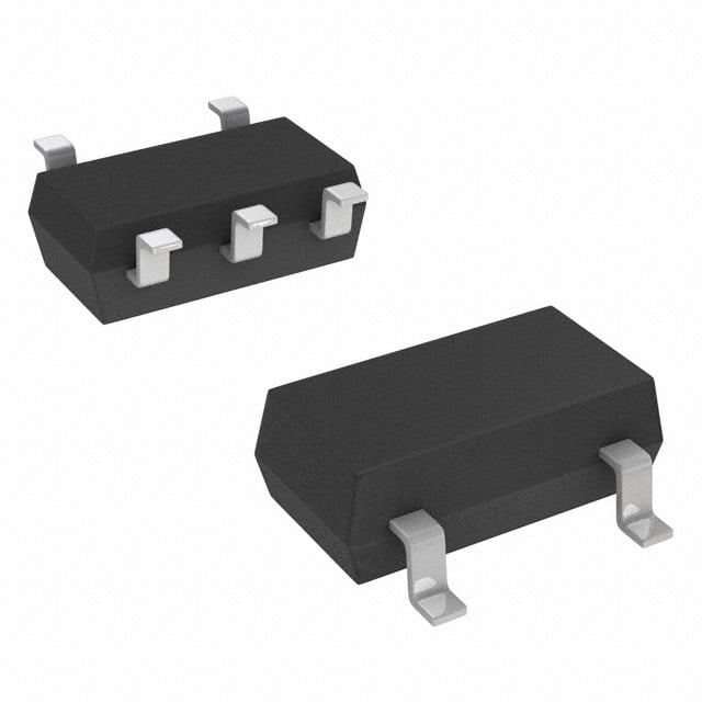
 Datasheet下载
- 型号: MAX4291EXK+T
- 制造商: Maxim
- 库位|库存: xxxx|xxxx
- 要求:
| 数量阶梯 | 香港交货 | 国内含税 |
| +xxxx | $xxxx | ¥xxxx |
查看当月历史价格
查看今年历史价格
MAX4291EXK+T产品简介:
ICGOO电子元器件商城为您提供MAX4291EXK+T由Maxim设计生产,在icgoo商城现货销售,并且可以通过原厂、代理商等渠道进行代购。 提供MAX4291EXK+T价格参考以及MaximMAX4291EXK+T封装/规格参数等产品信息。 你可以下载MAX4291EXK+T参考资料、Datasheet数据手册功能说明书, 资料中有MAX4291EXK+T详细功能的应用电路图电压和使用方法及教程。
MAX4291EXK+T是Maxim Integrated生产的一款低功耗、单电源供电的精密运算放大器,属于线性器件中的运算放大器类别。该器件具有微功耗、高精度和轨对轨输入/输出特性,适用于对功耗敏感且需要高精度信号处理的应用场景。

典型应用场景包括便携式医疗设备,如血糖仪、心率监测仪和可穿戴健康监测设备,其低功耗特性有助于延长电池寿命;工业传感器信号调理电路,如压力、温度或气体传感器,MAX4291EXK+T能够精确放大微弱信号,提高测量准确性;电池供电的数据采集系统中,用于模拟信号的前置放大和滤波处理;消费类电子产品,如智能手环、无线传感器节点等,得益于其小封装(SC70)和低静态电流(典型值为28μA),非常适合空间受限和节能要求高的设计。

此外,该运放具备宽工作电压范围(1.8V至5.5V)、低输入偏置电流和低失调电压,使其在精密检测和低噪声环境中表现优异。综上,MAX4291EXK+T广泛应用于便携式、低功耗、高精度模拟信号处理领域。
| 参数 | 数值 |
| -3db带宽 | - |
| 产品目录 | 集成电路 (IC)半导体 |
| 描述 | IC OPAMP GP 500KHZ RRO SC70-5运算放大器 - 运放 1.8V uPower Rail-Rail |
| 产品分类 | Linear - Amplifiers - Instrumentation, OP Amps, Buffer Amps集成电路 - IC |
| 品牌 | Maxim Integrated |
| 产品手册 | |
| 产品图片 |
|
| rohs | 符合RoHS无铅 / 符合限制有害物质指令(RoHS)规范要求 |
| 产品系列 | 放大器 IC,运算放大器 - 运放,Maxim Integrated MAX4291EXK+T- |
| 数据手册 | |
| 产品型号 | MAX4291EXK+T |
| 产品培训模块 | http://www.digikey.cn/PTM/IndividualPTM.page?site=cn&lang=zhs&ptm=25703http://www.digikey.cn/PTM/IndividualPTM.page?site=cn&lang=zhs&ptm=25705 |
| 产品目录页面 | |
| 产品种类 | 运算放大器 - 运放 |
| 供应商器件封装 | SC-70-5 |
| 共模抑制比—最小值 | 50 dB |
| 关闭 | No Shutdown |
| 其它名称 | MAX4291EXK+TDKR |
| 包装 | Digi-Reel® |
| 压摆率 | 0.2 V/µs |
| 商标 | Maxim Integrated |
| 增益带宽生成 | 0.5 MHz |
| 增益带宽积 | 500kHz |
| 安装类型 | 表面贴装 |
| 安装风格 | SMD/SMT |
| 封装 | Reel |
| 封装/外壳 | 6-TSSOP(5 引线),SC-88A,SOT-353 |
| 封装/箱体 | SC-70 |
| 工作温度 | -40°C ~ 85°C |
| 工作电源电压 | 1.8 V to 5.5 V, +/- 0.9 V to +/- 2.75 V |
| 工厂包装数量 | 2500 |
| 应用说明 | |
| 技术 | BiCMOS |
| 放大器类型 | 通用 |
| 最大双重电源电压 | +/- 2.75 V |
| 最大工作温度 | + 85 C |
| 最小双重电源电压 | +/- 0.9 V |
| 最小工作温度 | - 40 C |
| 标准包装 | 1 |
| 电压-电源,单/双 (±) | 1.8 V ~ 5.5 V, ±0.9 V ~ 2.75 V |
| 电压-输入失调 | 400µV |
| 电流-电源 | 100µA |
| 电流-输入偏置 | 15nA |
| 电流-输出/通道 | 20mA |
| 电源电流 | 100 uA |
| 电路数 | 1 |
| 系列 | MAX4291 |
| 转换速度 | 0.2 V/us |
| 输入偏压电流—最大 | 60 nA |
| 输入参考电压噪声 | 70 nV |
| 输入补偿电压 | 2.5 mV |
| 输出电流 | 20 mA |
| 输出类型 | 满摆幅 |
| 通道数量 | 1 Channel |
| 零件号别名 | MAX4291 |







- 商务部:美国ITC正式对集成电路等产品启动337调查
- 曝三星4nm工艺存在良率问题 高通将骁龙8 Gen1或转产台积电
- 太阳诱电将投资9.5亿元在常州建新厂生产MLCC 预计2023年完工
- 英特尔发布欧洲新工厂建设计划 深化IDM 2.0 战略
- 台积电先进制程称霸业界 有大客户加持明年业绩稳了
- 达到5530亿美元!SIA预计今年全球半导体销售额将创下新高
- 英特尔拟将自动驾驶子公司Mobileye上市 估值或超500亿美元
- 三星加码芯片和SET,合并消费电子和移动部门,撤换高东真等 CEO
- 三星电子宣布重大人事变动 还合并消费电子和移动部门
- 海关总署:前11个月进口集成电路产品价值2.52万亿元 增长14.8%





PDF Datasheet 数据手册内容提取
19-1612; Rev 3; 4/02 Ultra-Small, 1.8V, µPower, Rail-to-Rail I/O Op Amps M General Description Features A The MAX4291/MAX4292/MAX4294 family of micropow- (cid:2) Ultra-Low Voltage Operation—Guaranteed Down er operational amplifiers operates from a 1.8V to 5.5V X to 1.8V single supply or ±0.9V to ±2.75V dual supplies and has Rail-to-Rail® input/output capabilities. These amplifiers (cid:2) 100µA Supply Current per Amplifier 4 2 provide a 500kHz gain-bandwidth product and 120dB (cid:2) 500kHz Gain-Bandwidth Product open-loop voltage gain while using only 100µA of sup- 9 ply current per amplifier. The combination of low input (cid:2) 120dB Open-Loop Voltage Gain (RL= 100kΩ) 1 offset voltage (±200µV) and high open-loop gain makes (cid:2) 0.017% Total Harmonic Distortion Plus Noise / M them ideal for low-power/low-voltage, high-precision (THD + N) at 1kHz portable applications. A (cid:2) Rail-to-Rail Input Common-Mode Range The MAX4291/MAX4292/MAX4294 have an input com- X mon-mode range that extends to each supply rail, and (cid:2) Rail-to-Rail Output Drives 2kΩLoad their outputs swing to within 46mV of the rails with a 2kΩ 4 (cid:2) No Phase Reversal for Overdriven Inputs load. Although the minimum operating voltage is speci- 2 fied at 1.8V, these devices typically operate down to (cid:2) Unity-Gain Stable for Capacitive Loads up to 100pF 9 1.5V. The combination of ultra-low-voltage operation, rail- (cid:2) 200µV Input Offset Voltage (MAX4292/MAX4294) 2 to-rail inputs/output, and low-power consumption makes / these devices ideal for any portable/two-cell battery-pow- (cid:2) Single in Small 5-Pin SC70 M ered system. (cid:2) Available in Ultra-Small Packages: A The single MAX4291 is offered in an ultra-small 5-pin SC70 package. The dual MAX4292 is offered in a 5-Pin SC70 (MAX4291) X space-saving 8-bump, 1.5mm X 1.5mm footprint, ultra 8-Bump UCSP (MAX4292) 4 chip-scale package (UCSP™). 2 Ordering Information Applications 9 2-Cell Battery-Operated Systems PART TEMP RANGE PIN- TOP 4 PACKAGE MARK Portable Electronic Equipment MAX4291EXK-T -40°C to +85°C 5 SC70-5 AAD Battery-Powered Instrumentation MAX4291EUK-T -40°C to +85°C 5 SOT23-5 ADML Digital Scales MAX4292EBL-T* -40°C to +85°C 8 UCSP-8 AAJ Strain Gauges MAX4292EUA -40°C to +85°C 8 µMAX — Sensor Amplifiers MAX4292ESA -40°C to +85°C 8 SO — Cellular Phones MAX4294ESD -40°C to +85°C 14 SO — MAX4294EUD -40°C to +85°C 14 TSSOP — Pin Configurations *UCSP reliability is integrally linked to the user’s assembly methods, circuit board material, and environment. Refer to the TOP VIEW UCSP Reliability Notice in the UCSP Reliability section of this (BUMPS ON BOTTOM) data sheet for more information. OUTA VCC OUTB Selector Guide INA- MAX4292 INB- PART AMPLIFIERS PIN-PACKAGE MAX4291 1 5-pin SC70/SOT23 INA+ VEE INB+ MAX4292 2 8-pin µMAX/SO/UCSP MAX4294 4 14-pin SO/TSSOP UCSP Rail-to-Rail is a registered trademark of Nippon Motorola, Ltd. Pin Configurations continued at end of data sheet. UCSP is a trademark of Maxim Integrated Products, Inc. ________________________________________________________________Maxim Integrated Products 1 For pricing, delivery, and ordering information,please contact Maxim/Dallas Direct!at 1-888-629-4642, or visit Maxim’s website at www.maxim-ic.com.
Ultra-Small, 1.8V, µPower, Rail-to-Rail I/O Op Amps 4 ABSOLUTE MAXIMUM RATINGS 9 Supply Voltage (VCCto VEE)....................................................6V 8-Pin µMAX (derate 4.10mW/°C above +70°C)..............330mW 2 All Other Pins...................................(VCC+ 0.3V) to (VEE- 0.3V) 8-Pin SO (derate 5.88mW/°C above +70°C)..................471mW Current into IN_+, IN_-.....................................................±25mA 14-Pin SO (derate 8.33mW/°C above +70°C)................667mW 4 Output Short-Circuit Duration.....................................Continuous 14-Pin TSSOP (derate 6.3mW/°C above +70°C)............500mW X Continuous Power Dissipation (TA= +70°C) Operating Temperature Range............................-40°C to +85°C 5-Pin SC70 (derate 2.5mW/°C above +70°C)................200mW Junction Temperature......................................................+150°C A 5-Pin SOT23 (derate 7.1mW/°C above +70°C)................571mW Storage Temperature Range.............................-65°C to +150°C M 8-Bump UCSP (derate 4.7mW/°C above +70°C)...........379mW Lead Temperature (soldering, 10s).................................+300°C / 2 Stresses beyond those listed under “Absolute Maximum Ratings” may cause permanent damage to the device. These are stress ratings only, and functional operation of the device at these or any other conditions beyond those indicated in the operational sections of the specifications is not implied. Exposure to 9 absolute maximum rating conditions for extended periods may affect device reliability. 2 4 X ELECTRICAL CHARACTERISTICS A (VCC = 1.8V to 5.5V, VEE = VCM = 0, VOUT = VCC/2, RL = 100kΩ connected to VCC/2, TA = +25°C, unless otherwise noted.) (Note 1) M PARAMETER SYMBOL CONDITIONS MIN TYP MAX UNITS / 1 Supply Voltage Range VCC Inferred from PSRR test 1.8 5.5 V 9 Quiescent Supply Current VCC= 1.8V 100 210 2 (Per Amplifier) IQ VCC= 5.0V 100 255 µA 4 MAX4291 ±400 ±2500 X Input Offset Voltage VOS µV MAX4292/MAX4294 ±200 ±1200 A Input Bias Current IB VCC= 5.0V, 0 ≤VCM≤5.0V ±15 ±60 nA M Input Offset Current IOS VCC= 5.0V, 0 ≤VCM≤5.0V ±1 ±7 nA Differential Input Resistance RIN |VIN+- VIN-| < 10mV 0.75 MΩ Input Common-Mode Voltage VCM Inferred from CMRR test 0 VCC V Range Tested for MAX4291 50 80 0 ≤VCM≤ dB 1.8V; VCC= 1.8V MAX4292/MAX4294 57 80 Common-Mode Rejection Ratio CMRR Tested for MAX4291 60 90 0 ≤VCM≤ Common-Mode Rejection Ratio dB 5.0V, VCC= 5.0V MAX4292/MAX4294 66 90 Power-Supply Rejection Ratio PSRR 77 100 dB 2 _______________________________________________________________________________________
Ultra-Small, 1.8V, µPower, Rail-to-Rail I/O Op Amps ELECTRICAL CHARACTERISTICS (continued) M (VCC = 1.8V to 5.5V, VEE = VCM = 0, VOUT = VCC/2, RL = 100kΩ connected to VCC/2, TA = +25°C, unless otherwise noted.) A (Note 1) X PARAMETER SYMBOL CONDITIONS MIN TYP MAX UNITS 4 RL= 100kΩ, 0.02V ≤VOUT≤VCC- 0.02V 80 120 2 VCC= 1.8V 9 RL= 2kΩ, 1 80 110 0.1V ≤VOUT≤VCC- 0.1V / Large-Signal Voltage Gain AV dB M RL= 100kΩ, 0.02V ≤VOUT≤VCC- 0.02V 80 130 A VCC= 5.0V X RL= 2kΩ, 0.1V ≤VOUT≤VCC- 0.1V 80 120 4 2 Specified as RL= 100kΩto VCC/2 2 20 Output-Voltage Swing High VOH mV 9 |VCC- VOH| RL= 2kΩto VCC/2 15 40 2 Output-Voltage Swing Low VOL S|VpEeEc-i fVieOdL a|s RRLL== 120kΩ0ktΩo tVoC VCC/2C/2 4265 18200 mV /M Output Short-Circuit Current IOUT(SC) Sourcing or sinking 20 mA A Channel-to-Channel Isolation CHISO Specified at f = 10kHz (MAX4292/MAX4294 only) 83 dB X Gain-Bandwidth Product GBWP 500 kHz 4 Phase Margin φM 65 degrees 2 Gain Margin GM 12 dB 9 Slew Rate SR 0.2 V/µs 4 Input Voltage-Noise Density en f = 10kHz 70 nV/√Hz Input Current-Noise Density in f = 10kHz 0.05 pA/√Hz Capacitive-Load Stability AVCL= 1V/V,no sustained oscillations 100 pF ELECTRICAL CHARACTERISTICS (VCC= 1.8V to 5.5V, VEE= VCM= 0, VOUT= VCC/2, RL= 100kΩconnected to VCC/2, TA= TMINto TMAX, unless otherwise noted.) (Note 1) PARAMETER SYMBOL CONDITIONS MIN TYP MAX UNITS Supply-Voltage Range VCC Inferred from PSRR test 1.8 5.5 V Quiescent Supply Current VCC= 1.8V 240 IQ µA (Per Amplifier) VCC= 5.0V 270 MAX4291 ±3000 Input Offset Voltage VOS µV MAX4292/MAX4294 ±2000 _______________________________________________________________________________________ 3
Ultra-Small, 1.8V, µPower, Rail-to-Rail I/O Op Amps 4 ELECTRICAL CHARACTERISTICS (continued) 9 (VCC= 1.8V to 5.5V, VEE= VCM= 0, VOUT= VCC/2, RL= 100kΩconnected to VCC/2, TA= TMINto TMAX, unless otherwise noted.) 2 (Note 1) 4 PARAMETER SYMBOL CONDITIONS MIN TYP MAX UNITS X Input Offset Voltage Drift TCVOS 1.2 µV/°C A Input Bias Current IB VCC= 5.0V, 0 ≤VCM≤5.0V ±90 nA M Input Offset Current IOS VCC= 5.0V, 0 ≤VCM≤5.0V ±10 nA Input Common-Mode Voltage 2/ Range VCM Inferred from CMRR test 0 VCC V 9 Tested for MAX4291 50 2 0 ≤VCM≤1.8V, dB 4 VCC= 1.8V MAX4292/MAX4294 53 Common-Mode Rejection Ratio CMRR X Tested for MAX4291 60 A 0 ≤VCM≤5.0V, dB M VCC= 5.0V MAX4292/MAX4294 62 dB Power-Supply Rejection Ratio PSRR 75 dB / 1 RL= 100kΩ, 80 9 0.02V ≤VOUT≤VCC- 0.02V 2 VCC= 1.8V RL= 2kΩ, 80 4 0.1V ≤VOUT≤VCC- 0.1V X Large-Signal Voltage Gain AV dB RL= 100kΩ, 80 A 0.02V ≤VOUT≤VCC- 0.02V VCC= 5.0V M RL= 2kΩ, 80 0.1V ≤VOUT≤VCC- 0.1V Specified as RL= 100kΩto VCC/2 20 Output-Voltage Swing High VOH mV |VCC- VOH| RL= 2kΩto VCC/2 40 Specified as RL= 100kΩto VCC/2 80 Output-Voltage Swing Low VOL |VEE- VOL| RL= 2kΩto VCC/2 120 mV Note 1: All devices are 100% tested at TA= +25°C. All temperature limits are guaranteed by design. 4 _______________________________________________________________________________________
Ultra-Small, 1.8V, µPower, Rail-to-Rail I/O Op Amps Typical Operating Characteristics M (VCC= 2.4V, VEE= VCM= 0, VOUT= VCC/2, no load, TA= +25°C, unless otherwise noted.) A X SUPPLY CURRENT PER AMPLIFIER MINIMUM OPERATING VOLTAGE INPUT OFFSET VOLTAGE 4 vs. TEMPERATURE vs. TEMPERATURE (PSRR ≥ 80dB) vs. TEMPERATURE 2 µRENT (A) 111112354600000 VCC = 5.5V MAX4291 toc01 NG VOLTAGE (V) 11112.....67980 MAX4291 toc02 µOLTAGE (V)--3105000 VCC = 5.5V MAX4291 toc03 91/MA SUPPLY CUR 1189100000 VCC = 1.8V MINIMUM OPERATI 1111....2543 INPUT OFFSET V---674055000 VCC = 2.4VVCC = 1.8V X42 70 1.1 9 60 1.0 -900 2 -55-40-25-10 5 20 35 50 65 80 95 110125 -55-40-25-10 5 20 35 50 65 80 95 110125 -55-40-25-10 5 20 35 50 65 80 95110125 / TEMPERATURE (°C) TEMPERATURE (°C) TEMPERATURE (°C) M INPUT BIAS CURRENT INPUT BIAS CURRENT vs. INPUT BIAS CURRENT vs. A vs. TEMPERATURE COMMON-MODE VOLTAGE (VCC = 1.8V) COMMON-MODE VOLTAGE (VCC = 5.5V) X 3305 MAX4291 toc04 3400 MAX4291 toc05 3400 MAX4291 toc06 42 CURRENT (nA) 2205 VCC = 5.5V CURRENT (nA) 12000 CURRENT (nA) 12000 94 UT BIAS 15 UT BIAS -10 UT BIAS -10 INP 10 VCC = 1.8V INP -20 INP -20 5 -30 -30 0 -40 -40 -55-40-25-10 5 20 35 50 65 80 95110125 -0.5 0 0.5 1.0 1.5 2.0 2.5 -0.5 0.5 1.5 2.5 3.5 4.5 5.5 TEMPERATURE (°C) COMMON-MODE VOLTAGE (V) COMMON-MODE VOLTAGE (V) OUTPUT VOLTAGE SWING vs. OUTPUT VOLTAGE SWING vs. COMMON-MODE REJECTION RATIO TEMPERATURE (RL = 100kΩ TO VCC/2) TEMPERATURE (RL = 2kΩ TO VCC/2) vs. TEMPERATURE mV) 2350 VVOOHL == VVOCUCT - - V VOEUET MAX4291-07 mV) 5600 VVOOHL == VVOCUCT - - V VOEUET MAX4291-08 ---776055 0 ≤ VCM ≤ VCC VCC = 1.8V MAX4291 toc09 OUTPUT VOLTAGE SWING ( 1215005 VOH (VCC = 5.5V OR 1.8V) VVOOLL ( V(VCCCC = = 5 1.5.8VV)) OUTPUT VOLTAGE SWING ( 21430000 VOL (VCC = 1.8V) VOHV (OVLC C(V =C C5 .=5 V5).5V) CMRR (dB) ----99880550 VCC = 5.5V -100 VOH (VCC = 1.8V) 0 0 -105 -55 -25 5 35 65 95 125 -55 -25 5 35 65 95 125 -55-40-25-10 5 20 35 50 65 80 95110125 TEMPERATURE (°C) TEMPERATURE (°C) TEMPERATURE (°C) _______________________________________________________________________________________ 5
Ultra-Small, 1.8V, µPower, Rail-to-Rail I/O Op Amps 4 Typical Operating Characteristics (continued) 9 (VCC= 2.4V, VEE= VCM= 0, VOUT= VCC/2, no load, TA= +25°C, unless otherwise noted.) 2 4 X OPEN-LOOP GAIN vs. OUTPUT SWING LOW OPEN-LOOP GAIN vs. OUTPUT SWING HIGH OPEN-LOOP GAIN vs. OUTPUT SWING LOW (VCC = 1.8V, RL CONNECTED TO VCC) (VCC = 1.8V, RL CONNECTED TO VEE) (VCC = 5.5V, RL CONNECTED TO VCC) 2/MA 111123000 RRLL == 21kkΩΩ MAX4291 toc10 111102000 RRLL == 21kkΩΩ MAX4291 toc11 111123000 RL = 2kΩ RL = 1kΩ MAX4191 toc12 429 GAIN (dB) 1809000 GAIN (dB) 9800 GAIN (dB) 1809000 X 70 70 70 A 60 60 60 M 50 50 50 0 50 100 150 200 250 300 350 400 450 500 0 50 100 150 200 250 300 350 400 450 500 0 50 100 150 200 250 300 350 400 450 500 / 1 VOL (mV) VOH (mV) VOL (mV) 9 OPEN-LOOP GAIN vs. OUTPUT SWING HIGH MAX4292/MAX4294 2 (VCC = 5.5V, RL CONNECTED TO VEE) OPEN-LOOP GAIN vs. TEMPERATURE CROSSTALK vs. FREQUENCY AX4 111123000 RRLL == 21kkΩΩ MAX4191 toc13 111213000 MAX4291 toc14 --21000 MAX4291-15 M GAIN (dB) 1809000 PEN-LOOP GAIN (dB) 1890000 RL =R 2Lk =Ω 2 TkOΩ VTCOC VEE RL = 1RkLΩ = T1OkΩ V ETEO VCC CROSSTALK (dB) ----64530000 O 70 70 -70 60 60 -80 VCC = 5.5V 50 50 -90 0 50 100 150 200 250 300 350 400 450 500 -55-40-25-10 5 20 35 50 65 80 95110125 0.01 0.1 1 10 100 1000 VOH (mV) TEMPERATURE (°C) FREQUENCY (kHz) GAIN AND PHASE vs. FREQUENCY GAIN AND PHASE vs. FREQUENCY TOTAL HARMONIC DISTORTION (CL = 0) (CL = 100pF) PLUS NOISE vs. FREQUENCY 645000 AV = M1A0X04209V1 /toVc16 111840048 645000 AV = M1A0X04209V1 t/oVc17 111840048 1 R(CANLvOO ==NN F12IIVNkGΩ/VUVERRATTINIOGN) MAX4291 toc18 GAIN (dB) -231100000 70--3372662 PHASE (DEGREES)GAIN (dB) -231100000 73--0372662 PHASE (DEGREES) THD + NOISE (%) 0.1 VCC = 5.5V -20 -108 -20 -108 -30 -144 -30 -144 VCC = 1.8V -40 -180 -40 -180 0.01 0.1 1 10 100 1000 0.1 1 10 100 1000 0.01 0.1 1 10 100 FREQUENCY (kHz) FREQUENCY (kHz) FREQUENCY (kHz) 6 _______________________________________________________________________________________
Ultra-Small, 1.8V, µPower, Rail-to-Rail I/O Op Amps Typical Operating Characteristics (continued) M (VCC= 2.4V, VEE= VCM= 0, VOUT= VCC/2, no load, TA= +25°C, unless otherwise noted.) A X SMALL-SIGNAL TRANSIENT RESPONSE SMALL-SIGNAL TRANSIENT RESPONSE 4 LOAD RESISTOR vs. CAPACITIVE LOAD (NONINVERTING CONFIGURATION) (INVERTING CONFIGURATION) 2 100 1A(N0VO% =N 1OINVVV/EVERRSTHINOGO TCONFIGURATION) MAX4291 toc19 VVECEMCV A= C=X -4M 2229 ..=155 toVV0c20 100mV VVVCECECM = == - 220..55VV MAX4291 toc21 100mV 91 Ω) 10 IN IN /M R (k 0 0 O SIST 1 VCC = 5.5V A E AD R VCC = 2.4V 100mV 100mV X O L 4 0.1 OUT OUT 2 IVOCUCT => 52.05mVA IVOCUCT => 22.04mVA 0 0 9 0.01 2 0 1 2 3 4 5 6 7 8 9 10 1µs/div 1µs/div / CAPACITIVE LOAD (nF) M LARGE-SIGNAL TRANSIENT RESPONSE LARGE-SIGNAL TRANSIENT RESPONSE A (NONINVERTING CONFIGURATION) (INVERTING CONFIGURATION) X MAX4291 toc22 MAX4291 toc23 VCC = 2.5V VCC = 2.5V 4 VEE = -2.5V 2V VEE = -2.5V 2V VCM = 0 VCM = 0 2 9 IN IN -2V -2V 4 2V 2V OUT OUT -2V -2V 10µs/div 10µs/div SUPPLY CURRENT vs. SINK CURRENT SUPPLY CURRENT vs. SOURCE CURRENT 23500000 VCC = 5.5V MAX4291/2/4-24 111235050 VCC = 5.5V MAX4291/2/4-25 µA)2000 µA) 105 VCC = 2.4V NT ( NT ( 90 E E R R UR1500 UR 75 C C SUPPLY 1000 VCC = 2.4V SUPPLY 6405 VCC = 1.8V 30 500 VCC = 1.8V 15 0 0 0 5 10 15 20 25 30 0 5 10 15 20 25 SINK CURRENT (mA) SOURCE CURRENT (mA) _______________________________________________________________________________________ 7
Ultra-Small, 1.8V, µPower, Rail-to-Rail I/O Op Amps 4 Pin Description 9 PIN 2 MAX4292 NAME FUNCTION 4 MAX4291 MAX4294 µMAX/SO UCSP X 1 — — — IN+ Noninverting Input A Negative Supply. Connect to ground for M 2 4 C2 11 VEE single-supply operation. / 2 3 — — — IN- Inverting Input 9 4 — — — OUT Amplifier Output 2 4 5 8 A2 4 VCC Positive Supply X — 1, 7 A1, A3 1, 7 OUTA, OUTB Outputs for Amplifiers A and B A — 2, 6 B1, B3 2, 6 INA-, INB- Inverting Inputs to Amplifiers A and B M — 3, 5 C1, C3 3, 5 INA+, INB+ Noninverting Inputs to Amplifiers A and B / 1 — — — 8, 14 OUTC, OUTD Outputs for Amplifiers C and D 9 — — — 9, 13 INC-, IND- Inverting Inputs to Amplifiers C and D 2 — — — 10, 12 INC+, IND+ Noninverting Inputs to Amplifiers C and D 4 X Detailed Description A M Rail-to-Rail Input Stage IN MAX4291 MAX4292 The MAX4291/MAX4292/MAX4294 have rail-to-rail MAX4294 inputs and output stages that are specifically designed R3 for low-voltage, single-supply operation in the smallest package possible. The input stage consists of separate R3 = R1 R2 NPN and PNP differential stages, which operate togeth- er to provide a common-mode range extending to both supply rails. The crossover region of these two pairs R1 R2 occurs halfway between VCC and VEE. The input offset voltage is typically ±200µV (MAX4292/MAX4294). Low Figure 1a. Minimizing Offset Error Due to Input Bias Current operating supply voltage, low supply current, rail-to-rail (Noninverting) common-mode input range, and rail-to-rail outputs make this family of operational amplifiers (op amps) an excellent choice for precision or general-purpose, low- voltage, battery-powered systems. MAX4291 MAX4292 Since the input stage consists of NPN and PNP pairs, MAX4294 R3 the input bias current changes polarity as the common- mode voltage passes through the crossover region. Match the effective impedance seen by each input to R3 = R1 R2 reduce the offset error caused by input bias currents flowing through external source impedances (Figures IN 1a and 1b). R1 R2 The combination of high-source impedance plus input capacitance (amplifier input capacitance plus stray Figure 1b. Minimizing Offset Error Due to Input Bias Current (Inverting) 8 _______________________________________________________________________________________
Ultra-Small, 1.8V, µPower, Rail-to-Rail I/O Op Amps Table 1. MAX4291 Characteristics with Typical Battery Systems M MAX4291 A BATTERY TYPE RECHARGE- VFRESH VEND-OF-LIFE(V) CAPACITY, AA SIZE OPERATING TIME IN X ABLE (V) (mA-h) NORMAL MODE (h) 4 2 Alkaline (2 cells) No 3.0 1.8 2000 20,000 9 Nickel-Cadmium (2 cells) Yes 2.4 1.8 750 7500 1 / Lithium-Ion M Yes 3.5 2.7 1000 10,000 (1 cell) A Nickel-Metal- Yes 2.4 1.8 1000 10,000 X Hydride (2 cells) 4 2 IN+ VCC = 2.5V, VEE = -2.5V 10.6kΩ 9 IN 2 2.5V/div 0 / M A IN- X 10.6kΩ OUT 0 4 2.5V/div Figure 2. Input Protection Circuit 2 9 capacitance) creates a parasitic pole that produces an underdamped signal response. Reducing input capaci- 20µs/div 4 tance or placing a small capacitor across the feedback resistor improves response in this case. Figure 3. Rail-to-Rail Input/Output Voltage Range The MAX4291/MAX4292/MAX4294 family’s inputs are protected from large differential input voltages by inter- Rail-to-Rail Output Stage nal 10.6kΩ series resistors and back-to-back triple- The MAX4291/MAX4292/MAX4294 output stage can diode stacks across the inputs (Figure 2). For drive up to a 2kΩ load and still swing to within 46mV of differential input voltages (much less than 1.8V), input the rails. Figure 3 shows the output-voltage swing of a resistance is typically 0.75MΩ. For differential input MAX4291 configured as a unity-gain buffer, powered voltages greater than 1.8V, input resistance is around from a ±2.5V supply. The output for this setup typically 21.2kΩ, and the input bias current can be approximat- swings from (VEE + 25mV) to (VCC - 2mV) with a 100kΩ ed by the following equation: load. (V -1.8V) I = DIFF Applications Information BIAS 21.2kΩ Power-Supply Considerations In the region where the differential input voltage The MAX4291/MAX4292/MAX4294 operate from a sin- approaches 1.8V, the input resistance decreases expo- gle 1.8V to 5.5V supply (or dual ±0.9V to ±2.75V sup- nentially from 0.75MΩ to 21.2kΩ as the diode block plies) and consume only 100µA of supply current per begins to conduct. Conversely, the bias current amplifier. A high power-supply rejection ratio of 100dB increases with the same curve. allows the amplifiers to be powered directly off a In unity-gain configuration, high slew-rate input signals decaying battery voltage, simplifying design and may capacitively couple to the output through the triple- extending battery life. diode stacks. The MAX4291/MAX4292/MAX4294 are ideally suited for use with most battery-powered systems. Table 1 lists a _______________________________________________________________________________________ 9
Ultra-Small, 1.8V, µPower, Rail-to-Rail I/O Op Amps 4 MAX4291 OUTPUT SOURCE CURRENT 9 OFFSET VOLTAGE vs. SUPPLY VOLTAGE vs. TEMPERATURE 42 -450 TA = +85°C VCM = VCC/2 30 VCC = 5.5V VOH = VCC - VOUT X -500 mA) 25 VOH = 200mV VCC = 1.8V 92/MA µOFFSET VOLTAGE (V)---665055000 TA = +25°C TA = -40°C UTPUT SOURCE CURRENT ( 112500 VVCOCH == 55.05mVV VVCOVCHO ==H 11=.0 820V0m 0VmVVVVVCOCOCHCH ==== 1551.0.085m0VVmV V O 5 2 4 -700 0 X 0 0.5 1.0 1.5 2.0 2.5 3.03.5 4.0 4.5 5.0 5.5 -55-40-25-10 5 20 35 50 65 80 95110125 SUPPLY VOLTAGE (V) TEMPERATURE (°C) A Figure 4. Offset Voltage vs. Supply Voltage Figure 6a. Output Source Current vs. Temperature M / SUPPLY CURRENT PER AMPLIFIER OUTPUT SINK CURRENT 1 vs. SUPPLY VOLTAGE vs. TEMPERATURE 9 140 18 VCC = 5.5V VOL = VOUT - VEE 2 120 16 VOL = 200mV VCC = 5.5V MAX4 µSUPPLY CURRENT (A) 164800000 TA =T +A8 =5 °+C25°CTA = -40°C TPUT SINK CURRENT (mA) 11168024 VVCOCL == 150.50Vm V VVVCOOCL L == = 11 50.800Vmm VV VVVVCOCOCLCL ==== 521100..88m0VVmV V OU 4 20 2 0 0 0 0.5 1.0 1.5 2.0 2.5 3.03.5 4.0 4.5 5.05.5 -55-40-25-10 5 20 35 50 65 80 95110125 SUPPLY VOLTAGE (V) TEMPERATURE (°C) Figure 5. Supply Current per Amplifier vs. Supply Voltage Figure 6b. Output Sink Current vs. Temperature variety of typical battery types showing voltage when as a current source when driving the load toward VCC, fresh, voltage at end-of-life, capacity, and approximate and as a current sink when driving the load toward VEE. operating time from a MAX4291 (assuming nominal The limit of this current source/sink varies with supply conditions). voltage, ambient temperature, and lot-to-lot variations of the units. Although the amplifiers are fully guaranteed over tem- perature for operation down to a 1.8V single supply, Figures 6a and 6b show the typical current source and even lower voltage operation is possible in practice. sink capabilities of the MAX4291/MAX4292/MAX4294 Figures 4 and 5 show the offset voltage and supply cur- family as a function of supply voltage and ambient tem- rent as a function of supply voltage and temperature. perature. The contours on the graph depict the output current value, based on driving the output voltage to Load-Driving Capability within 50mV, 100mV, and 200mV of either power-sup- The MAX4291/MAX4292/MAX4294 are fully guaranteed ply rail. over temperature and supply voltage range to drive a maximum resistive load of 2kΩ to VCC/2, although For example, a MAX4291 running from a single 1.8V heavier loads can be driven in many applications. The supply, operating at TA = +25°C can source 3.5mA to rail-to-rail output stage of the amplifier can be modeled 10 ______________________________________________________________________________________
Ultra-Small, 1.8V, µPower, Rail-to-Rail I/O Op Amps M A 100mV X IN RISO 4 0 OUT 2 IN 9 MAX4291 RL CL 100mV 1 MAX4292 / MAX4294 OUT M 0 A 10µs/div X A V = R L R+L R IS O ≈ 1 VCC = 2.4V, RL = 2kΩ TO VEE, CL = 1000pF, RISO = 100Ω 4 2 Figure 7a. Using a Resistor to Isolate a Capacitive Load from Figure 7c. Pulse Response with Isolating Resistor (100Ω) 9 the Op Amp resistor between the output and the capacitive load 2 (Figure 7). Note that this alternative results in a loss of / M 100mV gain accuracy because RISO forms a voltage divider with the load resistor. A IN Power-Supply Bypassing and Layout X 0 The MAX4291/MAX4292/MAX4294 family operates from 4 either a single 1.8V to 5.5V supply or dual ±0.9V to 2 ±2.75V supplies. For single-supply operation, bypass 100mV 9 the power supply with a 100nF capacitor to VEE (in this case GND). For dual-supply operation, both the VCC 4 OUT 0 and the VEE supplies should be bypassed to ground with separate 100nF capacitors. 10µs/div Good PC board layout techniques optimize perfor- VCC = 2.4V, RL = 2kΩ TO VEE, CL = 1000pF mance by decreasing the amount of stray capacitance at the op amp’s inputs and output. To decrease stray capacitance, minimize trace lengths and widths by Figure 7b. Pulse Response Without Isolating Resistor placing external components as close as possible to within 100mV of VCC and is capable of driving a 485Ω the op amp. Surface-mount components are an excel- lent choice. load resistor to VEE: (1.8V − 0.1V) Using the MAX4291/MAX4292/MAX4294 RL = = 485Ω to VEE as Comparators 3.5mA Although optimized for use as operational amplifiers, The same application can drive a 220kΩ load resistor the MAX4291/MAX4292/MAX4294 can also be used as when terminated in VCC/2 (0.9V in this case). rail-to-rail I/O comparators. Typical propagation delay depends on the input overdrive voltage, as shown in Driving Capacitive Loads Figure 8. External hysteresis can be used to minimize The MAX4291/MAX4292/MAX4294 are unity-gain stable the risk of output oscillation. The positive feedback cir- for loads up to 100pF (see the Load Resistor vs. cuit, shown in Figure 9, causes the input threshold to Capacitive Load graph in the Typical Operating change when the output voltage changes state. The Characteristics). Applications that require greater two thresholds create a hysteresis band that can be capacitive-drive capability should use an isolation calculated by the following equations: ______________________________________________________________________________________ 11
Ultra-Small, 1.8V, µPower, Rail-to-Rail I/O Op Amps 4 PROPAGATION DELAY 9 vs. INPUT OVERDRIVE INPUT VHI HYSTERESIS 1000 2 VLO 4 VOH X tPD+, VCC = 5.5V OUTPUT VOL MA µ t (s)PD100 tPD-, VCtPCD =-, 5V.C5CV = t1P.D8+V, VCC = 1.8V VSIG R1 RVHCYCST / 2 VOUT 9 MAX4291 2 R2 VEE = GND MAX4292 4 10 VREF MAX4294 0 10 20 30 40 50 60 70 80 90 100 X VOD (mV) VEE = GND A Figure 8. Propagation Delay vs. Input Overdrive Figure 9. Hysteresis Comparator Circuit M 1/ VHYST = VHI − VLO MAXIMUM SvUsP.P SLUYP CPULRYR VEONLTT APGERE AMPLIFIER 9 R1 R1 12 2 V = 1 + + V COMPARATOR CONFIGURATION 4 HI R2 RHYST REF A) 10 VIN+ = (VIN-) - 100mV m AX VLO = VHI − RHRY1ST VCC URRENT ( 8 C M PLY 6 When the output of the comparator is low, the supply UP S current increases. The output stage has biasing circuit- M 4 U M ry to monitor the output current. When the amplifier is XI used as a comparator, the output stage is overdriven MA 2 and the current through the biasing circuitry increases 0 to maximum. For the MAX4291, typical supply currents 0 0.5 1.0 1.5 2.0 2.5 3.03.5 4.0 4.5 5.05.5 increase to 1.5mA with VCC = 1.8V and to 9mA when SUPPLY VOLTAGE (V) VCC= 5.0V (Figure 10). Figure 10. Maximum Supply Current per Amplifier vs. Supply Using the MAX4291/MAX4292/MAX4294 Voltage as Low-Power Current Monitors The MAX4291/MAX4292/MAX4294 are ideal for appli- emitter of the PNP transistor. Neglecting PNP base cur- cations powered from a two-cell battery stack. Figure rent, this current flows into R3, producing a ground-ref- 11 shows an application circuit in which the MAX4291 erenced voltage proportional to the load current. To is used for monitoring the current of a two-cell battery minimize errors, scale R1 to give a voltage drop that is stack. In this circuit, a current load is applied, and the large enough in comparison to the op amp’s VOS. voltage drop at the battery terminal is sensed. Calculate the output voltage of the application using The voltage on the load side of the battery stack is the following equation: equal to the voltage at the emitter of Q1 due to the feedback loop containing the op amp. As the load cur- R1 V = I × × R3 rent increases, the voltage drop across R1 and R2 OUT LOAD R2 increases. Thus, R2 provides a fraction of the load cur- rent (set by the ratio of R1 and R2) that flows into the 12 ______________________________________________________________________________________
Ultra-Small, 1.8V, µPower, Rail-to-Rail I/O Op Amps For a 1V output and a current load of 50mA, the choice M of resistors can be R1 = 2Ω, R2 = 100kΩ, and R3 = ILOAD 1MΩ. A R1 UCSP Information VCC X 4 Layout Issues R2 2 Design the layout for the IC to be as compact as possi- 9 ble to minimize parasitics. The UCSP uses a bump pitch of 0.5mm (19.7mil) and bump diameter of 0.3 1 Q1 (~12mil). Therefore, lay out the solder-pad spacing on / M 0.5mm (19.7mil) centers, using a pad size of 0.25mm VOUT (~10mil) and a solder mask opening of 0.33mm (13mil). A Round or square pads are permissible. Connect multi- X ple vias from the ground plane as close to the ground R3 pins as possible. MAX4291 4 Install capacitors as close as possible to the IC supply VEE 2 voltage pin. Place the ground end of these capacitors 9 Figure 11. Current Monitor for a 2-Cell Battery Stack near the IC GND pins to provide a low-impedance 2 return path for the signal current. / M Marking Information Prototype Chip Installation Alignment keys on the PC board, around the area A where the chip is located, will be helpful in the proto- X type assembly process. It is better to align the chip on ORIENTATION 4 the board before any other components are placed, PRODUCT ID CODE LOT CODE 2 and then place the board on a hot plate or hot surface until the solder starts melting. Remove the board from AAA 9 AAA the hot plate without disturbing the position of the chip 4 and let it cool down to room temperature before pro- cessing the board further. UCSP Reliability The UCSP represents a unique packaging form factor that may not perform as well as a packaged product through traditional mechanical reliability tests. UCSP reliability is integrally linked to the user’s assembly methods, circuit board material, and usage environ- ment. The user should closely review these areas when considering use of a UCSP. Performance through operating-life test and moisture resistance remains uncompromised. The wafer-fabrica- tion process primarily determines the performance. Mechanical stress performance is a greater considera- tion for UCSPs. UCSPs are attached through direct sol- der contact to the user’s PC board, foregoing the inherent stress relief of a packaged product lead frame. Solder-joint contact integrity must be considered. Comprehensive reliability tests have been performed and are available upon request. In conclusion, the UCSP performs reliably through environmental stresses. ______________________________________________________________________________________ 13
Ultra-Small, 1.8V, µPower, Rail-to-Rail I/O Op Amps 4 Pin Configurations (continued) 9 2 TOP VIEW 4 X OUTA 1 14 OUTD A INA- 2 13 IND- MAX4294 M INA+ 3 12 IND+ 2/ IN+ 1 5 VCC OUTA 1 8 VCC VCC 4 11 VEE 9 INA- 2 MAX4292 7 OUTB INB+ 5 10 INC+ MAX4291 2 VEE 2 INA+ 3 6 INB- INB- 6 9 INC- 4 IN- 3 4 OUT VEE 4 5 INB+ OUTB 7 8 OUTC X A SC70/SOT23 µMAX/SO TSSOP/SO M / 1 9 Chip Information 2 MAX4291 TRANSISTOR COUNT: 149 4 MAX4292 TRANSISTOR COUNT: 356 X MAX4294 TRANSISTOR COUNT: 747 A PROCESS: BiCMOS M 14 ______________________________________________________________________________________
Ultra-Small, 1.8V, µPower, Rail-to-Rail I/O Op Amps Package Information M (The package drawing(s) in this data sheet may not reflect the most current specifications. For the latest package outline information, A go to www.maxim-ic.com/packages.) X 4 SOT5L.EPS 2 9 1 / M A X 4 2 9 2 / M A X 4 2 9 4 SC70, 5L.EPS ______________________________________________________________________________________ 15
Ultra-Small, 1.8V, µPower, Rail-to-Rail I/O Op Amps 4 Package Information (continued) 9 (The package drawing(s) in this data sheet may not reflect the most current specifications. For the latest package outline information, 2 go to www.maxim-ic.com/packages.) 4 AX 8 4X S 8 DIM MIINNCHESMAX MMILINLIMETEMRASX 8LUMAXD.EPS M A - 0.043 - 1.10 A1 0.002 0.006 0.05 0.15 A2 0.030 0.037 0.75 0.95 / b 0.010 0.014 0.25 0.36 2 ÿ0.50±0.1 E H c 0.005 0.007 0.13 0.18 D 0.116 0.120 2.95 3.05 9 0.6±0.1 e 0.0256 BSC 0.65 BSC E 0.116 0.120 2.95 3.05 2 H 0.188 0.198 4.78 5.03 L 0.016 0.026 0.41 0.66 4 0.6±0.1 1 1 α 0∞ 6∞ 0∞ 6∞ X D BOTTOM VIEW S 0.0207 BSC 0.5250 BSC TOP VIEW A M A2 A1 A / 1 c α 9 e b L FRONT VIEW SIDE VIEW 2 4 X TPITRLOE:PRIETARY INFORMATION PACKAGE OUTLINE, 8L uMAX/uSOP A APPROVAL DOCUMENT CONTROL NO. REV. 1 21-0036 J 1 M Note: The MAX4292 does not have an exposed pad. OP.EPS TSS Note:The MAX4294 does not have an exposed pad. 16 ______________________________________________________________________________________
Ultra-Small, 1.8V, µPower, Rail-to-Rail I/O Op Amps Package Information (continued) M (The package drawing(s) in this data sheet may not reflect the most current specifications. For the latest package outline information, A go to www.maxim-ic.com/packages.) X 4 SOICN.EPS 29 1 / M A X 4 2 9 2 / M A X 4 2 9 4 ______________________________________________________________________________________ 17
Ultra-Small, 1.8V, µPower, Rail-to-Rail I/O Op Amps 4 Package Information (continued) 9 (The package drawing(s) in this data sheet may not reflect the most current specifications. For the latest package outline information, 2 go to www.maxim-ic.com/packages.) 4 X MA CSP, 3x3.EPS U / 9L 2 9 2 4 X A M / 1 9 2 4 X A M Maxim cannot assume responsibility for use of any circuitry other than circuitry entirely embodied in a Maxim product. No circuit patent licenses are implied. Maxim reserves the right to change the circuitry and specifications without notice at any time. 18 ____________________Maxim Integrated Products, 120 San Gabriel Drive, Sunnyvale, CA 94086 408-737-7600 © 2002 Maxim Integrated Products Printed USA is a registered trademark of Maxim Integrated Products.
Mouser Electronics Authorized Distributor Click to View Pricing, Inventory, Delivery & Lifecycle Information: M axim Integrated: MAX4291EUK+T MAX4291EUK-T MAX4291EXK+T MAX4291EXK-T MAX4292ESA MAX4292ESA+ MAX4292ESA+T MAX4292EUA MAX4292EUA+ MAX4292EUA+T MAX4294ESD+ MAX4294ESD+T MAX4294EUD+ MAX4294EUD+T MAX4292ESA-T MAX4292EUA-T MAX4292EBL-T MAX4292EBL+T