ICGOO在线商城 > MAX8630WETD20+T

 Datasheet下载
- 型号: MAX8630WETD20+T
- 制造商: Maxim
- 库位|库存: xxxx|xxxx
- 要求:
| 数量阶梯 | 香港交货 | 国内含税 |
| +xxxx | $xxxx | ¥xxxx |
查看当月历史价格
查看今年历史价格
MAX8630WETD20+T产品简介:
ICGOO电子元器件商城为您提供MAX8630WETD20+T由Maxim设计生产,在icgoo商城现货销售,并且可以通过原厂、代理商等渠道进行代购。 提供MAX8630WETD20+T价格参考以及MaximMAX8630WETD20+T封装/规格参数等产品信息。 你可以下载MAX8630WETD20+T参考资料、Datasheet数据手册功能说明书, 资料中有MAX8630WETD20+T详细功能的应用电路图电压和使用方法及教程。
MAX8630WETD20+T是Maxim Integrated推出的一款专用LED驱动器,属于PMIC(电源管理集成电路)中的LED驱动器类别。该芯片采用高效的电荷泵架构,专为驱动白光LED而设计,常用于需要背光照明的便携式电子设备。

其典型应用场景包括智能手机、平板电脑、手持终端和小型LCD显示屏的背光驱动。由于该器件支持多LED并行驱动,并具备恒流输出特性,能够确保各LED亮度均匀,提升显示效果。它还集成了软启动、过温保护、开路/短路保护等安全功能,提高了系统可靠性。

MAX8630WETD20+T采用紧凑的晶圆级封装(WLP),占用PCB空间小,非常适合对尺寸敏感的便携式产品。其低噪声电荷泵设计减少了对外部滤波元件的需求,有助于简化电路设计、降低成本。此外,芯片支持I²C或PWM调光控制方式,可实现精确的亮度调节,适用于需要多级亮度控制的应用环境。

综上,MAX8630WETD20+T广泛应用于移动消费类电子产品中,尤其适合要求高效率、小体积和高可靠性的LED背光驱动场景。
| 参数 | 数值 |
| 产品目录 | 集成电路 (IC) |
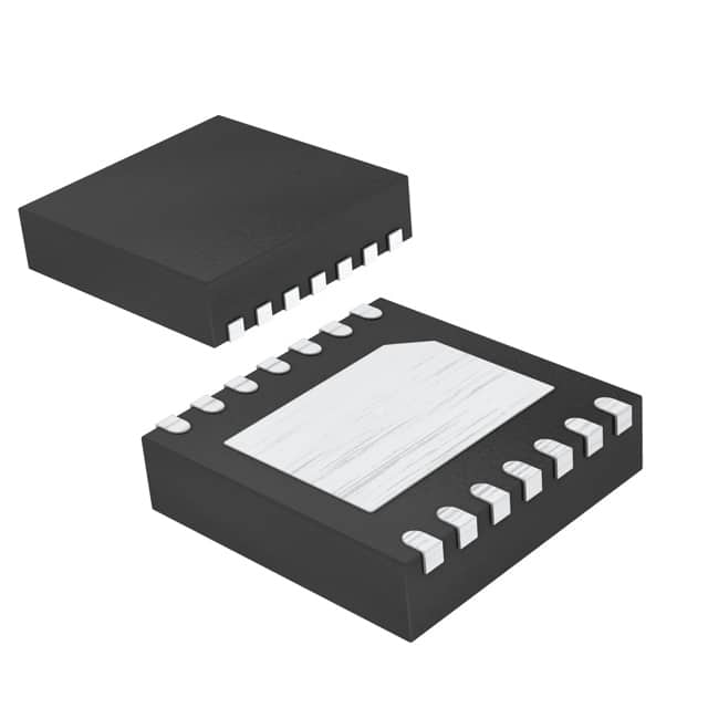
| 描述 | IC LED DRVR WHITE BCKLGT 14TDFN |
| 产品分类 | |
| 品牌 | Maxim Integrated |
| 数据手册 | |
| 产品图片 |
|
| 产品型号 | MAX8630WETD20+T |
| rohs | 无铅 / 符合限制有害物质指令(RoHS)规范要求 |
| 产品系列 | - |
| 产品培训模块 | http://www.digikey.cn/PTM/IndividualPTM.page?site=cn&lang=zhs&ptm=25703http://www.digikey.cn/PTM/IndividualPTM.page?site=cn&lang=zhs&ptm=25705 |
| 供应商器件封装 | 14-TDFN-EP(3x3) |
| 其它名称 | MAX8630WETD20+TDKR |
| 内部驱动器 | 是 |
| 包装 | Digi-Reel® |
| 安装类型 | 表面贴装 |
| 封装/外壳 | 14-WFDFN 裸露焊盘 |
| 工作温度 | -40°C ~ 85°C |
| 应用说明 | |
| 恒压 | - |
| 恒流 | 是 |
| 拓扑 | PWM,切换式电容器(充电泵) |
| 标准包装 | 1 |
| 电压-电源 | 2.7 V ~ 5.5 V |
| 电压-输出 | - |
| 类型-初级 | 背光 |
| 类型-次级 | 白色 LED |
| 输出数 | 5 |
| 频率 | 1MHz |










PDF Datasheet 数据手册内容提取
19-0825; Rev 0; 5/07 EVAALVUAAILTAIOBNL EKIT 125mA 1x/1.5x Charge Pumps for 5 White LEDs in 3mm x 3mm TDFN General Description Features M The MAX8630W/MAX8630X charge pumps drive up to 5 ♦ 93% Max/85% Avg. Efficiency (PLED/PBATT) Over A white LEDs with regulated constant current up to 125mA Li+ Battery Discharge X total. By utilizing adaptive 1x/1.5x charge-pump modes ♦ 1% LED Current Accuracy and very low-dropout current regulators, they achieve ♦ 125mA Total Drive Capability 8 high efficiency over the full 1-cell Li+ battery input volt- ♦ Adaptive 1x/1.5x Mode Switchover 6 age range. The 1MHz fixed-frequency switching allows for tiny external components, and the regulation scheme ♦ Single-Wire, Serial-Pulse Dimming (MAX8630X) 3 is optimized to ensure low EMI and low input ripple. An Independent On/Off/Dimming for Main and Sub 0 integrated derating function protects the LEDs from Linear—Full, 31/32nd, 30/32nd, … 1/32nd W overheating during high ambient temperatures. ♦ Direct-PWM Dimming (MAX8630W) / The MAX8630W/MAX8630X are factory trimmed for full- ♦ 15, 18, 20, and 25mA Full-Scale Versions M scale LED current options of 15mA, 18mA, 20mA, and ♦ Low 0.1µA Shutdown Current A 25mA. The MAX8630X uses two enable inputs (ENM for ♦ Soft-Start Eliminates Inrush Current 3 main LEDs and ENS for 2 sub LEDs) for simple on/off X ♦ Output Overvoltage Protection control and single-wire, serial-pulse dimming in 32 linear 8 steps. The MAX8630W uses a single direct PWM input ♦ Thermal-Derating Function Protects LEDs 6 (PWM) to control all 5 LEDs with DC current proportional ♦ 14-Pin, 3mm x 3mm TDFN Package 3 to the PWM duty cycle. If both ENM and ENS (or PWM) are kept low for more than 4ms, the MAX8630_ enters Ordering Information 0 shutdown. The MAX8630W/MAX8630X are available in a X 14-pin, 3mm x 3mm TDFN package (0.8mm max height). PART PIN- TOP PKG PACKAGE MARK CODE Applications 14 TDFN-14 MAX8630WETD15+T ADQ T1433-2 Display Backlight (Up to 5 LEDs) (3mm x 3mm) Main (3 LEDs) + Sub (2 LEDs) Displays Note:All devices are specified to operate over the -40°C to +85°C operating temperature range. Cell Phones and Smartphones +Denotes a lead-free package. PDAs, Digital Cameras, and Camcorders T = Tape and reel. Ordering Information continuedat end of data sheet. Selector Guide appears at end of data sheet. Typical Operating Circuit Pin Configuration 1μF TOP VIEW WM) M) P W INPUT ED1 ED2 ED3 ED4 ED5 NM (C NS (P 2.7V TO 5.5V C1P C1N OUTPUT L L L L L E E IN OUT 14 13 12 11 10 9 8 1μF 1μF GND MAX8630X MAIN LED1 MAX8630W ENABLE MAIN LED2 MAX8630X ON/OFF AND ENM LED3 DIMMING SUB LED4 ENABLE SUB ON/OFF AND ENS LED5 1 2 3 4 5 6 7 DIMMING C2P C2N D N N N P P T GN C1 I C2 C2 C1 OU TDFN 1μF 3mm × 3mm ( ) ARE FOR MAX8630W ________________________________________________________________Maxim Integrated Products 1 For pricing, delivery, and ordering information,please contact Maxim/Dallas Direct!at 1-888-629-4642, or visit Maxim’s website at www.maxim-ic.com.
125mA 1x/1.5x Charge Pumps for 5 White LEDs in 3mm x 3mm TDFN X ABSOLUTE MAXIMUM RATINGS 0 IN, OUT to GND.....................................................-0.3V to +6.0V Continuous Power Dissipation (TA= +70°C) C1N, C2N, ENM, CPWM, ENS, 14-Pin TDFN 3mm x 3mm 3 PWM to GND............................................-0.3V to (VIN+ 0.3V) (derate 18.2mW/°C above +70°C).............................1454mW 6 LED_ to GND............................................-0.3V to (VOUT+ 0.3V) Junction Temperature......................................................+150°C 8 C1P, C2P to GND...-0.3V to greater of (VOUT+ 1V) or (VIN+ 1V) Storage Temperature Range.............................-65°C to +150°C OUT Short Circuit to GND..........................................Continuous Lead Temperature (soldering, 10s).................................+300°C X A Stresses beyond those listed under “Absolute Maximum Ratings” may cause permanent damage to the device. These are stress ratings only, and functional operation of the device at these or any other conditions beyond those indicated in the operational sections of the specifications is not implied. Exposure to M absolute maximum rating conditions for extended periods may affect device reliability. / W ELECTRICAL CHARACTERISTICS 0 (VIN= 3.6V, VGND= 0V, EN_ (PWM) = IN, TA= -40°C to +85°C, unless otherwise noted. Typical values are at TA= +25°C.) (Note 1) 3 PARAMETER CONDITIONS MIN TYP MAX UNITS 6 IN Operating Voltage 2.7 5.5 V 8 X Undervoltage-Lockout Threshold VIN rising or falling 2.20 2.45 2.65 V Undervoltage-Lockout Hysteresis 100 mV A Output Overvoltage Protection M VOUT rising, any LED_ = GND 5 V Threshold 1/32nd setting, 1.5x mode 1.4 No-Load Supply Current mA 1/32nd setting, 1x mode 0.35 TA = +25°C 0.01 2 Shutdown Supply Current ENM = ENS (PWM) = GND µA TA = +85°C 0.1 Soft-Start Time (tSOFT-START) 2 ms MAX8630_ETD15 15 MAX8630_ETD18 18 Full-Scale LED Current mA MAX8630_ETD20 20 MAX8630_ETD25 25 TA = +25°C -1 ±0.3 +1 Full-Scale LED Current Accuracy % TA = -40°C to derating function start temperature -3.5 ±0.3 +3.5 Derating Function Start 40 °C Temperature Derating Function Slope TA = +40°C to +85°C -1.67 %/°C LED_ Dropout Voltage 100% LED setting (Note 2) 40 75 mV 1x to 1.5x Mode Transition VLED_ falling 88 mV Threshold Input Voltage Mode Transition 70 mV Hysteresis 1.5x Mode Regulation Voltage Minimum of VLED_ 122 mV OUT Pulldown Resistance in ENM = ENS (PWM) = GND 5 kΩ Shutdown 2 _______________________________________________________________________________________
125mA 1x/1.5x Charge Pumps for 5 White LEDs in 3mm x 3mm TDFN ELECTRICAL CHARACTERISTICS (continued) M (VIN= 3.6V, VGND= 0V, EN_ (PWM) = IN, TA= -40°C to +85°C, unless otherwise noted. Typical values are at TA= +25°C.) (Note 1) A PARAMETER CONDITIONS MIN TYP MAX UNITS X Open-Loop OUT Resistance 1x mode, (VIN - VOUT) / IOUT 0.8 1.5 Ω 8 1.5x mode, (1.5VIN - VOUT) / IOUT 3.2 7.2 6 Maximum OUT Current VIN ≥ 3.2V, VOUT = 3.9V 125 mA 3 OUT Short-Circuit Current Limit VOUT < 1.25V 57 mA 0 Switching Frequency 1 MHz W Direct-PWM Dimming Filter CCPWM = 0.1µF, (PWM frequency of 900Hz to 200kHz 10 Hz / Corner Frequency (MAX8630W) recommended) M EN_ (PWM) High Voltage VIN = 2.7V to 5.5V 1.4 V A EN_ (PWM) Low Voltage VIN = 2.7V to 5.5V 0.4 V X EN_ (PWM) Minimum Input VIN = 2.7V to 5.5V (recommended minimum slew rate) 1 V/µs 8 Slew Rate 6 TA = +25°C 0.01 1 EN_ (PWM) Input Current VEN_ (PWM) = 0V or 5.5V µA 3 TA = +85°C 0.1 0 EN_ (PWM) Low Shutdown Delay X 4 ms (tSHDN) EN_ tLO (See Figure 4) 0.5 500.0 µs EN_ tHI (See Figure 4) 0.5 µs Initial EN_ tHI (See Figure 4) First EN_ (PWM) high pulse 50 µs Thermal Shutdown +160 °C Thermal-Shutdown Hysteresis 20 °C Note 1:Limits are 100% production tested at TA= +25°C. Limits over the operating temperature range are guaranteed by design. Note 2:Dropout voltage is defined as the LED_ to GND voltage at which current into LED_ drops 10% from the value at VLED_= 0.2V. Typical Operating Characteristics (VIN= 3.6V, ENM = ENS = IN, TA= +25°C, unless otherwise noted.) EFFICIENCY vs. INPUT VOLTAGE INPUT CURRENT vs. INPUT VOLTAGE INPUT CURRENT vs. INPUT VOLTAGE DRIVING 5 LEDs DRIVING 5 LEDs DRIVING 3 MAIN LEDs 100 160 160 90 W/X toc01 140 VIN FALLING W/X toc02 140 VIN FALLING W/X toc03 7800 MAX8630 A) 120 ILED = 20mA MAX8630 A) 120 ILED = 20mA MAX8630 EFFICIENCY (%) 34560000 ILED = 1.875mAILED = 8.125mIALED = 20mA INPUT CURRENT (m 146800000 ILILEEDD = = 1 8.8.17255mmAA INPUT CURRENT (m 146800000 ILED = 8.125mA 20 ILED = 1.875mA 20 20 10 VIN FALLING 0 0 0 2.7 3.0 3.3 3.6 3.9 4.2 2.7 3.0 3.3 3.6 3.9 4.2 2.7 3.0 3.3 3.6 3.9 4.2 INPUT VOLTAGE (V) INPUT VOLTAGE (V) INPUT VOLTAGE (V) _______________________________________________________________________________________ 3
125mA 1x/1.5x Charge Pumps for 5 White LEDs in 3mm x 3mm TDFN X Typical Operating Characteristics (continued) 0 (VIN= 3.6V, ENM = ENS = IN, TA= +25°C, unless otherwise noted.) 3 6 INPUT CURRENT vs. INPUT VOLTAGE INPUT RIPPLE VOLTAGE vs. SUPPLY LED CURRENT MATCHING vs. INPUT 8 DRIVING 2 SUB LEDs VOLTAGE DRIVING 5 WHITE LEDs VOLTAGE (25mA/LED) 30W/MAX INPUT CURRENT (mA) 111146820460000000 IILLEEDD == 82.01m25AmA VIN FALLING MAX8630W/X toc04 PUT RIPPLE VOLTAGE (mV)P-P 111468024000000 2280m1mm5AAmA//L/ALLEE/EDLDDED MAX8630W/X toc05 LED CURRENT (mA) 22222222345678 MAX8630W/X toc06 6 IN 8 20 ILED = 1.875mA 20 21 X 0 0 20 2.7 3.0 3.3 3.6 3.9 4.2 2.7 3.2 3.7 4.2 2.7 3.1 3.5 3.9 4.3 4.7 5.1 5.5 A INPUT VOLTAGE (V) INPUT VOLTAGE (V) INPUT VOLTAGE (V) M LED CURRENT MATCHING vs. INPUT OUTPUT CURRENT vs. TEMPERATURE VOLTAGE (2.5mA/LED) (5 LEDs AT 25mA EACH) 2.80 140 LED CURRENT (mA) 22222.....3456700000 MAX8630W/X toc07 OUTPUT CURRENT (mA) 114680200000 TDEEMRAPTEIRNAGTURE MAX8630W/X toc08 2.20 2.10 20 2.00 0 2.7 3.1 3.5 3.9 4.3 4.7 5.1 5.5 -40 -15 10 35 60 85 INPUT VOLTAGE (V) TEMPERATURE (°C) 1x MODE OPERATING WAVEFORMS 1.5x MODE OPERATING WAVEFORMS (VIN = 4.0V) (VIN = 3.6V) MAX8630W/X toc09 MAX8630W/X toc10 200mV/div 200mV/div VOUT (AC-COUPLED) VOUT (AC-COUPLED) 200mV/div 200mV/div VIN (AC-COUPLED) VIN (AC-COUPLED) IIN 100mA/div IIN 100mA/div 1μs/div 1μs/div 4 _______________________________________________________________________________________
125mA 1x/1.5x Charge Pumps for 5 White LEDs in 3mm x 3mm TDFN Typical Operating Characteristics (continued) M (VIN= 3.6V, ENM = ENS = IN, TA= +25°C, unless otherwise noted.) A X MAIN STARTUP AND SHUTDOWN 8 STARTUP AND SHUTDOWN WITH SUB ENABLED 6 MAX8630W/X toc11 MAX8630W/X toc12 5V/div 5V/div 3 VENM AND 0 VENM 0 0 VENS VOUT 2V/div W 2V/div / M VOUT 0 0 100mA/div 100mA/div A IIN IIN 0 0 X 100mA/div 100mA/div 8 0 IOUT IOUT 0 6 1ms/div 1ms/div 3 0 LINE-TRANSIENT RESPONSE WITH MODE CHANGE X STARTUP AND DIMMING (VIN = 3.8V TO 3.2V TO 3.8V) MAX8630W/X toc13 MAX8630W/X toc14 VENM AND 5V/div VIN 1V/div VENS 1V/div VOUT 500mV/div VOUT 0 50mA/div IOUT IOUT 20mA/div 0 20ms/div 200μs/div Pin Description PIN N AM E F UN CT IO N M AX 86 30 X M AX 86 30 W G ro und. Co nnect GN D to system g r ound and the in p ut by pa ss cap acit or as 1 1 G ND clo se to the IC as po ssi b le . Co nnect GN D to the expo sed pa d d ir ectl y und er the IC. Tra nsfer C ap aci tor 1 Ne g ati ve C onnectio n. C onnect a 1µF cera m ic cap aci tor 2 2 C 1N fro m C1 P to C 1N . S up pl y Vo l tag e Inpu t. Co nnect a 1µF cer am ic capa cit or fr om IN to GN D . The 3 3 IN i np ut volt ag e r ange is 2.7V to 5.5V. Tra nsfer C ap aci tor 2 Ne g ati ve C onnectio n. C onnect a 1µF cera m ic cap aci tor 4 4 C 2N fro m C2 P to C 2N . _______________________________________________________________________________________ 5
125mA 1x/1.5x Charge Pumps for 5 White LEDs in 3mm x 3mm TDFN X Pin Description (continued) 0 PIN 3 N AM E F UN CT IO N M AX 86 30 X M AX 86 30 W 6 Tra nsfer C ap aci tor 2 Po si ti ve C onnectio n. C onnect a 1µF cera m ic cap aci tor 8 5 5 C 2P fro m C2 P to C 2N . X Tra nsfer C ap aci tor 1 Po si ti ve C onnectio n. C onnect a 1µF cera m ic cap aci tor A 6 6 C 1P fro m C1 P to C 1N . M O utpu t. Co nnect a 1µF cera m ic capa ci tor fro m O UT to G ND . C onnect OUT to / 7 7 OU T the anod es of all the LED s. In shutdo wn , OUT i s pu l le d d ow n b y an i ntern al W 5kΩ r esi stor . 0 E nabl e and D i mm in g C ontr ol for S ub LE Ds ( LE D 4 and LED 5) . D ri ve EN S l og ic - 3 l ow for gr eater than 4ms to di s abl e the sub LE Ds . Dr i ve bo th EN M and E NS 6 l og ic -l ow for g re ater than 4ms to shut do wn the IC. D ri ve EN S l og ic - hi gh to 8 b eg in soft-s tar t and enab le m axi mu m ( 100% ) sub LE D curr ent. Su b sequ ent 8 — E NS X p ul ses on EN S cause the sub LED curr ent to de cre ase i n 32 li near steps . Because of the soft- star t d el ay, it is po ssi bl e to turn on the IC and qu i ckly set a A d im l evel so the sub LED curr ent never tr ansit io ns thro ugh the ma xi m um M setti ng . S ee the E NM /E NS Di mm i ng C ontro l sectio n. E nabl e and D i mm in g C ontr ol for Ma i n LED s (L E D1 , LED 2, and LE D 3) . Dr i ve E NM l og i c- lo w for g r eater than 4ms to di s ab l e the m ai n LED s. Dr iv e bo th E NM and E NS lo gi c-l ow for gr eater than 4m s to shut do wn the IC . D ri ve E N M lo g ic - hig h to be gi n soft- start and enabl e m axim um (1 00% ) ma in LE D curr e nt. 9 — EN M S ub sequ ent pu ls es on E NM cause the m ain LED curr ent to de cre ase i n 32 l in ear steps . Because of the soft-s tart de l ay, i t is po ssi bl e to turn on the IC and q ui ckly set a d im l evel so the ma i n LED cur r ent never tr ansi tio ns thro ug h the m axim um setti ng . Se e the E NM /E NS Di mm i ng C ontro l sectio n. D ir ect P WM i npu t. PW M contro l s outpu t cur re nt as a pe rc entage of full - scale — 8 P WM cur re nt in p r op or ti on to PW M sig nal d uty cycle . The fre q uency r ange is 900H z to 200kH z. P WM Fil ter C apa ci tor C onnecti on. C onnect a capa ci tor fr om CP W M to G N D to — 9 C PW M for m a fil ter w it h the in tern al 150kΩ r esis tor . The r ecomm end ed cap aci tor for 10H z cor ner i s 0.1µF. 10 10 LED 5 S ub LED Ca thode C onnecti ons and Ch ar g e- Pu mp Feed b ack. Cu rr ent flo wi ng i nto LE D _ is ba sed on the EN S ( or PW M ) de scr ip ti on abo ve. The charg e p um p r eg ul ates the lo w est LED _ vol tag e to 0.12V. Co nnect LED _ to OU T i f the 11 11 LED 4 cor re sp ond in g LED i s not po pu la ted . 12 12 LED 3 M ai n LE D C athod e Co nnectio ns and C har ge -P um p Feed ba ck. Cu r re nt flo w i ng i nto LE D _ is ba sed on the EN M ( or PW M ) de scr ip ti on abo ve. The charg e p um p 13 13 LED 2 r eg ul ates the lo w est LED _ vol tag e to 0.12V. Co nnect LED _ to OU T i f the 14 14 LED 1 cor re sp ond in g LED i s not po pu la ted . — — E P E xp osed Pa dd l e. Co nnect to GND d ir ectly und er the IC. 6 _______________________________________________________________________________________
125mA 1x/1.5x Charge Pumps for 5 White LEDs in 3mm x 3mm TDFN 1μF 1μF M A C1P C1N C1P C1N X 2.7V TO 5.5V 2.7V TO 5.5V IN OUT IN OUT 8 1μF 1μF 1μF 1μF 6 GND GND MAX8630X MAIN MAX8630W 3 LED1 LED1 0 ENABLE MAIN LED2 CPWM LED2 W ON/OFF AND ENM LED3 0.1μF LED3 SERIAL DIMMING / SUB M LED4 LED4 ENABLE SUB DIRECT PWM A ON/OFF AND ENS LED5 PWM LED5 SIGNAL SERIAL DIMMING C2P C2N C2P C2N X 8 1μF 1μF 6 3 Figure 1. Typical Applications Circuit with the MAX8630X Figure 2. Typical Applications Circuit with the MAX8630W 0 X C1 C2 1μF 1μF C1P C1N C2P C2N INPUT 2.7V TO 5.5V IN 1x/1.5x REGULATING OUT CHARGE PUMP 1CμINF C1μOUFT GND ERROR MAX8630W AMP 1 MAX8630X OVD 1.25V ENS CONTROL AND (PWM) REFERENCE MIN 0.12V SELECT ENM SUB CONTROL (CPWM) MAIN CONTROL 0.6V LED1 D1 LED2 D2 MAX8630W ONLY LED3 D3 LED4 D4 LED5 D5 ERROR AMP 2 0.6V + + + + + – – – – – RSET ( ) ARE FOR MAX8630W Figure 3. Functional Diagram _______________________________________________________________________________________ 7
125mA 1x/1.5x Charge Pumps for 5 White LEDs in 3mm x 3mm TDFN X Detailed Description and the LED output current is then ramped up in 32 lin- ear steps. If the current regulators are in dropout at the 0 The MAX8630_ charge pump drives up to 5 white LEDs end of this time, the charge pump switches to 1.5x (3 main LEDs and 2 sub LEDs) with regulated constant 3 mode. If the output is shorted to ground (VOUT < current for uniform intensity. By utilizing adaptive 1x/1.5x 6 1.25V), the part stays in the initial soft-start stage and charge-pump modes and very low-dropout current regu- 8 output current is limited by the ramped current source. lators, it achieves 125mA guaranteed output-drive capa- Additionally, when the main or sub LED current rolls X bility and high efficiency over the 1-cell Li+ battery input over from 1/32 to full, the LED current regulators soft- A voltage range. 1MHz fixed-frequency switching allows start again to eliminate input current spikes. M for tiny external components and the regulation scheme ENM/ENS Dimming Control (MAX8630X) is optimized to ensure low EMI and low input ripple. The W/ MAX8630X provides independent on/off/dimming control When the LEDs are enabled (by driving EN_ high), the MAX8630X goes through soft-start and brings the LED for main and sub displays (see Figure 1). The current up in 32 linear steps. Dim the MAX8630X by puls- 0 MAX8630W allows direct-PWM dimming of all five LEDs ing EN_ low (500ns to 500µs pulse width). Each pulse 3 together (see Figure 2). A functional diagram for the reduces the LED current by 1/32nd. After 31 pulses, the 6 MAX8630X/MAX8630W is shown in Figure 3. current reaches 1/32, and the next pulse restores the cur- 8 1x to 1.5x Switchover rent to 100%. Figure 4 shows a timing diagram for EN_. X When VIN is higher than VOUT, the MAX8630_ operates If dimming control is not required, ENM and ENS work A in 1x mode and VOUT is pulled up to VIN. The internal as simple on/off controls. Drive ENM/ENS high to current regulators regulate the LED current. As VIN enable the LEDs, or drive ENM/ENS low for shutdown. M drops, VLEDMIN_ eventually falls below the switchover The LEDs operate at 100% brightness under these sim- threshold of 88mV, and the MAX8630_ starts switching ple on/off conditions. in 1.5x mode, and VLEDMIN is regulated to 122mV by PWM Dimming Control (MAX8630W) the charge pump. To switch back to 1x mode, the MAX8630_ determines if VIN- VOUTis sufficient to keep Dim the MAX8630W by applying a direct-PWM logic- VLEDMIN greater than 88mV. The comparator that level signal to PWM. An internal resistor combined with makes this judgment is adaptive and matches the the capacitor at CPWM forms a lowpass filter that con- switchover for the conditions. verts the PWM signal to DC LED current that is propor- tional to the PWM signal’s duty cycle. All five LEDS are Soft-Start controlled together on the MAX8630W. The PWM fre- The MAX8630_ includes soft-start circuitry to eliminate quency range is 900Hz to 200kHz. inrush current at turn-on. When starting up, the output If dimming control is not required, PWM works as a sim- capacitor is charged directly from the input with a ple on/off control. Drive PWM high to enable the LEDs, ramped current source (with no charge-pump action) or drive PWM low for shutdown. until the output voltage approaches the input voltage. Once this occurs, the charge pump enters 1x mode, 0 1 2 3 4 5 27 28 29 30 31 32 INITIAL tHI EN_ > 50μs FULtLSOFT-START 31/32 30/32 29/325002n8s/3 T2O 52070/μ3ts2LO >5t0H0Ins FULL 31/32 tS4HmDsN ILED_ 6/32 5/32 4/32 3/32 SHUTDOWN 2/32 1/32 SHUTDOWN Figure 4. MAX8630X EN_ Timing Diagram 8 _______________________________________________________________________________________
125mA 1x/1.5x Charge Pumps for 5 White LEDs in 3mm x 3mm TDFN Shutdown Mode Applications Information M When both ENM and ENS (or PWM) are held low for 4ms or longer, the MAX8630_ is shut down and put in a Driving Fewer than 5 LEDs A low-current mode. OUT is internally pulled to GND with To avoid overvoltage protection mode when using X 5kΩduring shutdown. fewer than five LEDs, connect any unused LED_ to 8 OUT. The MAX8630_ contains special circuitry to Overvoltage Protection detect this condition and disables the corresponding 6 If any LED fails as an open circuit, the corresponding current regulator to avoid wasting battery current. 3 VLED_ goes to 0V, and the output voltage is limited to 0 about 5V by gating on/off the charge pump. In case Input Ripple any LED_ is floating or grounded, the MAX8630_ oper- For LED drivers, input ripple is more important than out- W ates in the same overvoltage protection mode. To avoid put ripple. Input ripple depends on the source supply’s / overvoltage protection mode when using fewer than output impedance. Adding a lowpass filter to the input M five LEDs, connect any unused LED_ to OUT. The of the MAX8630_ further reduces input ripple. A MAX8630_ contains special circuitry to detect this con- Alternatively, increasing CIN to 2.2µF (or 4.7µF) cuts dition and disables the corresponding current regulator input ripple in half (or in fourth) with only a small X to avoid wasting battery current. increase in footprint. The 1x mode always has very low 8 input ripple. Thermal Shutdown 6 The MAX8630_ includes a thermal-protection circuit Component Selection 3 that shuts down the IC when the die temperature reach- Ceramic capacitors are recommended due to their 0 es about +160°C. The part turns on after the IC cools small size, low cost, and low ESR. Select ceramic X by approximately 20°C. capacitors that maintain their capacitance over temper- ature and DC bias. Capacitors with X5R or X7R temper- Temperature Derating Function ature characteristics generally perform well. See Table The MAX8630 contains a derating function that auto- 1 for a list of recommended components. Using a larg- matically limits the LED current at high temperatures in er value input capacitor helps to reduce input ripple accordance with the recommended derating curve of (see the Input Ripple section). popular white LEDs. The derating function enables the safe usage of higher LED currents at room tempera- PCB Layout and Routing ture, thus reducing the number of LEDs required to The MAX8630_ is a high-frequency, switched-capacitor backlight the display. The derating circuit protects the voltage regulator. For best circuit performance, use a LEDs from overheating at high PCB temperatures. The solid ground plane and place CIN, COUT, C1, and C2 derating circuit limits the LED current by reducing the as close to the MAX8630_ as possible. See the internal 600mV reference voltage above +40°C at MAX8630_ evaluation kit for an example layout. approximately -1.67%/°C. The typical derating function Chip Information characteristic is shown in the Typical Operating Characteristics. PROCESS: BiCMOS Table 1. Recommended Components DESIGNATION VALUE MANUFACTURER PART NUMBER DESCRIPTION Taiyo Yuden JMK105 BJ105MV 1µF ±20%, 6.3V X5R ceramic capacitors (0402) CIN, COUT, C1, C2 1µF TDK C1005X5R0J105M 1µF ±20%, 6.3V X5R ceramic capacitors (0402) D1–D5 — Nichia NSCW215T White LEDs _______________________________________________________________________________________ 9
125mA 1x/1.5x Charge Pumps for 5 White LEDs in 3mm x 3mm TDFN X Ordering Information (continued) Selector Guide 0 PIN- TOP PKG FULL-SCALE DIMMING PART PART 3 PACKAGE MARK CODE CURRENT (mA) INTERFACE 6 14 TDFN-14 MAX8630WETD18+T ADR T1433-2 MAX8630WETD15 15 Direct PWM 8 (3mm x 3mm) MAX8630WETD18 18 Direct PWM X 14 TDFN-14 MAX8630WETD20+T ADS T1433-2 MAX8630WETD20 20 Direct PWM (3mm x 3mm) A MAX8630WETD25 25 Direct PWM 14 TDFN-14 M MAX8630WETD25+T (3mm x 3mm) ADT T1433-2 MAX8630XETD15 15 Serial Pulse / 14 TDFN-14 MAX8630XETD18 18 Serial Pulse W MAX8630XETD15+T ADU T1433-2 (3mm x 3mm) MAX8630XETD20 20 Serial Pulse 0 14 TDFN-14 MAX8630XETD25 25 Serial Pulse MAX8630XETD18+T ADV T1433-2 (3mm x 3mm) 3 6 MAX8630XETD20+T 14 TDFN-14 ADW T1433-2 (3mm x 3mm) 8 14 TDFN-14 X MAX8630XETD25+T ADX T1433-2 (3mm x 3mm) A Note:All devices are specified to operate over the -40°C to M +85°C operating temperature range. +Denotes a lead-free package. T = Tape and reel. 10 ______________________________________________________________________________________
125mA 1x/1.5x Charge Pumps for 5 White LEDs in 3mm x 3mm TDFN Package Information M (The package drawing(s) in this data sheet may not reflect the most current specifications. For the latest package outline information A go to www.maxim-ic.com/packages.) X S 8 P N.E 6 HI 3 T N 0 F D W L, 0 1 / & M 8, 6, A X 8 6 3 0 X ______________________________________________________________________________________ 11
125mA 1x/1.5x Charge Pumps for 5 White LEDs in 3mm x 3mm TDFN X Package Information (continued) 0 (The package drawing(s) in this data sheet may not reflect the most current specifications. For the latest package outline information go to www.maxim-ic.com/packages.) 3 6 8 X COMMON DIMENSIONS PACKAGE VARIATIONS A SYMBOL MIN. MAX. PKG. CODE N D2 E2 e JEDEC SPEC b [(N/2)-1] x e M A 0.70 0.80 T633-2 6 1.50±0.10 2.30±0.10 0.95 BSC MO229 / WEEA 0.40±0.05 1.90 REF / D 2.90 3.10 T833-2 8 1.50±0.10 2.30±0.10 0.65 BSC MO229 / WEEC 0.30±0.05 1.95 REF W E 2.90 3.10 T833-3 8 1.50±0.10 2.30±0.10 0.65 BSC MO229 / WEEC 0.30±0.05 1.95 REF A1 0.00 0.05 T1033-1 10 1.50±0.10 2.30±0.10 0.50 BSC MO229 / WEED-3 0.25±0.05 2.00 REF 0 L 0.20 0.40 T1033-2 10 1.50±0.10 2.30±0.10 0.50 BSC MO229 / WEED-3 0.25±0.05 2.00 REF 3 k 0.25 MIN. T1433-1 14 1.70±0.10 2.30±0.10 0.40 BSC - - - - 0.20±0.05 2.40 REF 6 A2 0.20 REF. T1433-2 14 1.70±0.10 2.30±0.10 0.40 BSC - - - - 0.20±0.05 2.40 REF 8 X A M Maxim cannot assume responsibility for use of any circuitry other than circuitry entirely embodied in a Maxim product. No circuit patent licenses are implied. Maxim reserves the right to change the circuitry and specifications without notice at any time. 12 ____________________Maxim Integrated Products, 120 San Gabriel Drive, Sunnyvale, CA 94086 408-737-7600 © 2007 Maxim Integrated Products is a registered trademark of Maxim Integrated Products, Inc.
Mouser Electronics Authorized Distributor Click to View Pricing, Inventory, Delivery & Lifecycle Information: M axim Integrated: MAX8630WETD20+T MAX8630WETD25+T MAX8630XETD20+T MAX8630XETD15+T