ICGOO在线商城 > MAX9921AUB+
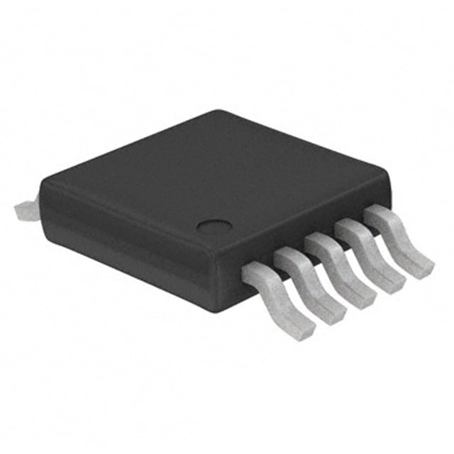
 Datasheet下载
- 型号: MAX9921AUB+
- 制造商: Maxim
- 库位|库存: xxxx|xxxx
- 要求:
| 数量阶梯 | 香港交货 | 国内含税 |
| +xxxx | $xxxx | ¥xxxx |
查看当月历史价格
查看今年历史价格
MAX9921AUB+产品简介:
ICGOO电子元器件商城为您提供MAX9921AUB+由Maxim设计生产,在icgoo商城现货销售,并且可以通过原厂、代理商等渠道进行代购。 提供MAX9921AUB+价格参考以及MaximMAX9921AUB+封装/规格参数等产品信息。 你可以下载MAX9921AUB+参考资料、Datasheet数据手册功能说明书, 资料中有MAX9921AUB+详细功能的应用电路图电压和使用方法及教程。
MAX9921AUB+是Maxim Integrated推出的一款霍尔效应传感器接口IC,专为汽车和工业应用中的速度和位置检测设计。其典型应用场景包括车轮转速感应(如防抱死制动系统ABS)、变速箱速度检测、发动机凸轮轴/曲轴位置监测等。该芯片可接收来自霍尔传感器的模拟信号,经过内部信号调理和比较器处理后,输出精确的数字脉冲信号,适用于恶劣环境下的高可靠性需求。MAX9921AUB+具备宽工作电压范围、高抗电磁干扰能力和故障诊断功能,适合在高温、高振动的汽车环境中稳定运行。此外,它也广泛用于工业电机控制、旋转编码器和各类非接触式位置检测系统中,提升系统精度与安全性。
| 参数 | 数值 |
| 产品目录 | 集成电路 (IC)半导体 |
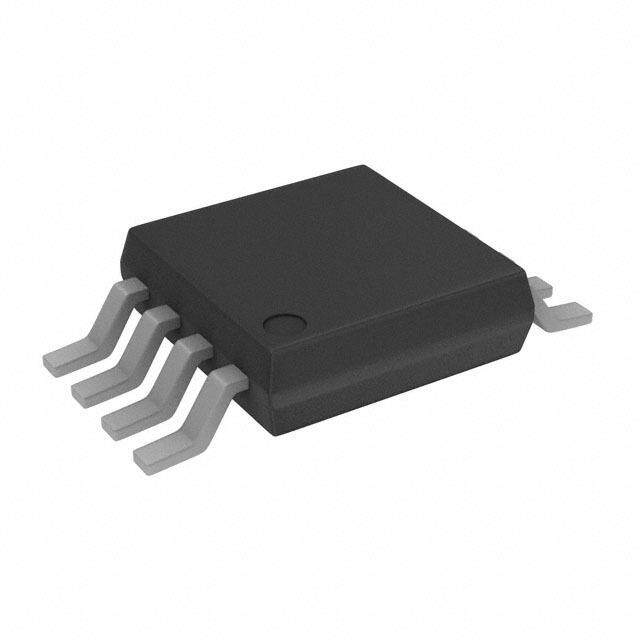
| 描述 | IC SENSOR HALL EFFECT 10-MSOP接口 - 专用 Dual Hall-Effect Sensor Interface |
| 产品分类 | |
| 品牌 | Maxim Integrated |
| 产品手册 | |
| 产品图片 |
|
| rohs | 符合RoHS无铅 / 符合限制有害物质指令(RoHS)规范要求 |
| 产品系列 | 接口 IC,接口 - 专用,Maxim Integrated MAX9921AUB+- |
| 数据手册 | |
| 产品型号 | MAX9921AUB+ |
| 产品培训模块 | http://www.digikey.cn/PTM/IndividualPTM.page?site=cn&lang=zhs&ptm=25703http://www.digikey.cn/PTM/IndividualPTM.page?site=cn&lang=zhs&ptm=25705 |
| 产品种类 | |
| 产品类型 | Dual, 2-Wire Hall-Effect Sensor Interface with Diagnostics |
| 供应商器件封装 | 10-uMAX |
| 包装 | 管件 |
| 商标 | Maxim Integrated |
| 安装类型 | 表面贴装 |
| 安装风格 | SMD/SMT |
| 封装 | Tube |
| 封装/外壳 | 10-TFSOP,10-MSOP(0.118",3.00mm 宽) |
| 封装/箱体 | UMAX-10 |
| 工作电源电压 | 6 V to 18 V |
| 工厂包装数量 | 50 |
| 应用说明 | |
| 接口 | 2 线 |
| 最大功率耗散 | 444.4 mW |
| 最大工作温度 | + 125 C |
| 最小工作温度 | - 40 C |
| 标准包装 | 1 |
| 电流-电源 | 1.3mA |
| 电源电流 | 1 mA |
| 类型 | 霍尔效应传感器 |
| 系列 | MAX9921 |
| 输入类型 | 电压 |
| 输出类型 | 逻辑 |
| 零件号别名 | MAX9921 |





- 商务部:美国ITC正式对集成电路等产品启动337调查
- 曝三星4nm工艺存在良率问题 高通将骁龙8 Gen1或转产台积电
- 太阳诱电将投资9.5亿元在常州建新厂生产MLCC 预计2023年完工
- 英特尔发布欧洲新工厂建设计划 深化IDM 2.0 战略
- 台积电先进制程称霸业界 有大客户加持明年业绩稳了
- 达到5530亿美元!SIA预计今年全球半导体销售额将创下新高
- 英特尔拟将自动驾驶子公司Mobileye上市 估值或超500亿美元
- 三星加码芯片和SET,合并消费电子和移动部门,撤换高东真等 CEO
- 三星电子宣布重大人事变动 还合并消费电子和移动部门
- 海关总署:前11个月进口集成电路产品价值2.52万亿元 增长14.8%


PDF Datasheet 数据手册内容提取
19-4119; Rev 1; 1/10 EVAALVUAAILTAIOBNL EKIT Dual, 2-Wire Hall-Effect Sensor Interface with Diagnostics General Description Features M The MAX9921 provides a single chip solution to interface (cid:2) Withstands 60V at BAT Supply and Hall Inputs A two 2-wire Hall-effect sensors to a low-voltage micro- (cid:2) 6V to 18V Operating Voltage Range X processor (µP). This device supplies and monitors the cur- (cid:2) Provides Supply Current and Interfaces to Two rent drawn by two Hall-effect sensors, filters the sensed 9 2-Wire Hall Sensors current level, and outputs the corresponding logic level. 9 (cid:2) Error Output with Diagnostics of Hall Inputs and The MAX9921 includes input diagnostics and fault pro- BAT Voltage 2 tection. These features allow the device to determine fault (cid:2) Protects Hall Sensors from Overvoltage by 1 conditions such as open inputs, inputs shorted to the bat- Isolating Them from Supply Transients tery, and inputs shorted to ground. If the MAX9921 detects any of these conditions at either IN1 or IN2, the (cid:2) Hall Inputs Protected from Short to Ground device shuts off the current to the corresponding input. (cid:2) Ramps Current to Hall Sensors at 4mA/µs The MAX9921 protects the Hall sensors from supply tran- (cid:2) Output Enable Input Allows Multiplexing of sients up to 60V at the BAT supply. Normal operating Outputs from Multiple MAX9921s supply voltage ranges from 6V to 18V. If the battery volt- (cid:2) Hall Output Filtering age is out of range, the MAX9921 shuts off the current to (cid:2) Hall Sensor Blanking Following Hall Sensor the Hall sensors. Power-Up or Restart The MAX9921 provides an 80µs blanking time following (cid:2) Low-Power Shutdown, Controlled with OE and Hall sensor power-up or restart. The open-drain logic DIAG Inputs outputs are compatible with logic levels up to 5.5V. (cid:2) Operates with ±2V Ground Shifts Between Hall The MAX9921 is available in a small 10-pin µMAX® Sensor and MAX9921 package and is specified over the -40°C to +125°C Ordering Information automotive temperature range. Applications PART TEMP RANGE PIN-PACKAGE MAX9921AUB+T -40°C to +125°C 10 µMAX Door Modules Powered Lift Gate MAX9921AUB/V+T -40°C to +125°C 10 µMAX Controllers Window Lifters +Denotes a lead(Pb)-free/RoHS-compliant package. Powered Running Boards Seat Movers T = Tape and reel. Seatbelt Buckles /V denotes an automotive qualified part. Electric Sunroofs Pin Configuration appears at end of data sheet. Typical Application Circuit WVBIATTH: S6TVA TNOD S18 6V0 VOPERATING, RISET = 63.4kΩ, 1% 0.1μF 3.3V TO 5V BAT BATTERY ISET 10kΩ E C REF N U DGIEANGENROASTTIOICNS, OE VCC AND CONTROL S C OVERVOLTAGE ERR O DETECT REMOTE NN 0.01μF DIAG μP/LOGIC GROUND E IN1 CIRCUIT OUT1 C FILTER N T 0.01μF O IN2 MAX9921 S R FILTER OUT2 GND GND REMOTE GROUND µMAX is a registered trademark of Maxim Integrated Products, Inc. ________________________________________________________________Maxim Integrated Products 1 For pricing, delivery, and ordering information,please contact Maxim Directat 1-888-629-4642, or visit Maxim’s website at www.maxim-ic.com.
Dual, 2-Wire Hall-Effect Sensor Interface with Diagnostics 1 ABSOLUTE MAXIMUM RATINGS 2 BAT to GND............................................................-0.3V to +60V Current into IN1, IN2.......................................................±100mA 9 ISET to BAT...........................................................-2.0V to +0.3V Continuous Power Dissipation (TA= +70°C) 9 IN1, IN2 to GND..........-5.0V to the lower of +60V or (VBAT+ 1V) 10-Pin µMAX (derate 5.6mW/°C above +70°C).........444.4mW DIAG, OE to GND..................................................-0.3V to +6.0V Operating Temperature Range.........................-40°C to +125°C X OUT1, OUT2, ERRto GND....................................-0.3V to +6.0V Junction Temperature......................................................+150°C A Short-Circuit Duration of OUT1, OUT2, ERRto GND Storage Temperature Range.............................-65°C to +150°C or to 5.5V (individually)............................................Continuous Lead Temperature (soldering, 10s).................................+300°C M Current into Any Pin Except IN1, IN2...............................±20mA Stresses beyond those listed under “Absolute Maximum Ratings” may cause permanent damage to the device. These are stress ratings only, and functional operation of the device at these or any other conditions beyond those indicated in the operational sections of the specifications is not implied. Exposure to absolute maximum rating conditions for extended periods may affect device reliability. DC ELECTRICAL CHARACTERISTICS (VBAT= 13.6V, VDIAG= 0, VOE= 5V, IN1 = IN2 = no connection, RISET= 63.4kΩ, RPU= 10kΩat ERR, OUT1 and OUT2, TA= -40°C to +125°C, unless otherwise noted. Typical values are at TA= +25°C.) (Note 1) PARAMETER SYMBOL CONDITIONS MIN TYP MAX UNITS GENERAL BAT Supply Range VBAT 6 18 V VBAT Low for ERR Output Active VBL 5.2 V VBAT High for ERR Output Active VBH 22 V IBAT Normal mode 1 1.3 mA BAT Supply Current ISD Shutdown mode, VOE = VDIAG = 0V 1 µA HALL INPUTS (IN1 and IN2) RISET = 63.4kΩ -11.5 Input Current for Output High IIH mA RISET = 59.0kΩ -12.4 RISET = 63.4kΩ -7.2 Input Current for Output Low IIL mA RISET = 59.0kΩ -7.8 Input Current Hysteresis for RISET = 63.4kΩ 0.76 IIN,HYS mA High/Low Detection RISET = 59.0kΩ 0.78 Input Pullup Impedance RPU VBAT = 6V, inputs IN1, IN2 with 50 Ω IIN = -14mA Input Voltage Interpreted as VSB Measured with respect to VBAT 100 mV Shorted to Battery Current Range Interpreted as IOC -2 +0.02 mA Open Circuit Current Level Interpreted as Not a sustained RISET = 63.4kΩ -23 ISC condition, reverts to - mA Shorted Sensor to Ground 50µA when detected RISET = 59.0kΩ -25 2 _______________________________________________________________________________________
Dual, 2-Wire Hall-Effect Sensor Interface with Diagnostics DC ELECTRICAL CHARACTERISTICS (continued) M (VBAT= 13.6V, VDIAG= 0, VOE= 5V, IN1 = IN2 = no connection, RISET= 63.4kΩ, RPU= 10kΩat ERR, OUT1 and OUT2, TA= -40°C A to +125°C, unless otherwise noted. Typical values are at TA= +25°C.) (Note 1) X PARAMETER SYMBOL CONDITIONS MIN TYP MAX UNITS 9 LOGIC I/O (OUT1, OUT2, ERR, DIAG, and OE) 9 Output Voltage Low (ERR, OUT1, VOL Sink current = 1mA 0.4 V 2 OUT2) 1 Three-State Output Current (ERR, IOZ VOE = 0V, 0 ≤ VOUT_ ≤ 5V ±1 µA OUT1, OUT2) Input-Voltage High (DIAG, OE) VIH 2.1 V Input-Voltage Low (DIAG, OE) VIL 0.8 V Input Resis tance to GND (D I AG, OE) RIN 50 80 kΩ AC TIMING CHARACTERISTICS (VBAT= 13.6V, VDIAG= 0, VOE= 5V, IN1 = IN2 = no connection, RISET= 63.4kΩ, RPU = 10kΩat ERR, OUT1 and OUT2, TA= -40°C to +125°C, unless otherwise noted. Typical values are at TA= +25°C.) (Notes 1, 2, and 4) PARAMETER SYMBOL CONDITIONS MIN TYP MAX UNITS IN1, IN2 Blanking Time at Hall IIH = -11.5mA to GND, time from VIN_ = tBL 50 140 µs Switch Power-Up 500mV until OUT_ high, CL = 20pF (Note 3) IN1, IN2 Current Ramp Rate tRAMP VIN = GND 3.8 mA/µs After Turn-On Delay from IN_ to OUT_ (Filter From IIH to IIL or from IIL to IIH, CL = 20pF, tDEL 6.5 µs Delay) Figure 1 From IIL to ISC or from IIH to IOC, falling edge Delay from IN_ Fault to ERR tERR 31 ns only, CL = 20pF, Figure 1 Delay from DIAG High to Rising edge of DIAG to falling or rising edge tDLH 350 ns OUT_ and ERR of outputs, CL = 20pF, Figure 1 Delay from DIAG Low to OUT_ Falling edge of DIAG to falling or rising edge tDHL 1.6 µs and ERR of outputs, CL = 20pF, Figure 1 Delay Difference Between CHALL-BYPASS = 0.01µF, IIH = -11.5mA and Rising and Falling Edges for tDM 20 ns IIL = -7.2mA, CL = 20pF Both Channels Delay Difference Between CHALL-BYPASS = 0.01µF, IIH = -11.5mA and tCC 100 ns Channels IIL = -7.2mA, CL = 20pF Maximum Frequency on Hall CHALL-BYPASS = 0.01µF, IIH = -11.5mA and fMAX 50 kHz Inputs IIL = -7.2mA, CL = 20pF IN_ Pulse Length Rejected by PR Figure 2 5.5 µs Filter to OUT_ Note 1: All DC specifications are 100% tested at TA= +25°C. AC specifications and specifications over -40°C to +125°C are guar- anteed by design. Note 2: CLis external load capacitance on the outputs for test only. Note 3: These blanking times apply when the MAX9921 is operating in normal mode. Blanking times following power-up or startup from shutdown mode are 20µs longer. Note 4: The following AC parameters change with the value of RISET: tBL, tRAMP, tDEL, fMAX, and PR. The typ values given are for RISET= 63.4kΩ. The parameters tRAMPand fMAXincrease 8%, and tDELand PRdecrease 8% with RISET= 59.0kΩ. The lim- its for tBLand fMAXapply for both resistor values. _______________________________________________________________________________________ 3
Dual, 2-Wire Hall-Effect Sensor Interface with Diagnostics 1 Timing Diagrams 2 9 9 APPROX. 50mA X RETRY A SHORT CIRCUIT M 14mA IN 1 7mA 4mA/μs HALL SENSOR OPEN CIRCUIT 0mA tDEL 5V OUT1 0V 5V OUT2 0V tERR tERR 5V ERR 0V 5V DIAG 0V Figure 1. Timing Diagram 4 _______________________________________________________________________________________
Dual, 2-Wire Hall-Effect Sensor Interface with Diagnostics Timing Diagrams (continued) M A X 9 PR PR 9 2 14mA 1 IN_ 7mA 0mA tDEL tDEL 5V OUT_ 0V Figure 2. Hall Input Pulse Rejection _______________________________________________________________________________________ 5
Dual, 2-Wire Hall-Effect Sensor Interface with Diagnostics 1 Typical Operating Characteristics 2 (VBAT= 14V, TA= +25°C, unless otherwise noted.) 9 9 BAT SUPPLY CURRENT BAT SUPPLY CURRENT BAT SUPPLY CURRENT X vs. VBAT IN OPERATING MODE vs. VBAT IN OPERATING MODE vs. VBAT IN OPERATING MODE MA 11..34 TA = -40°C MAX9921 toc01 11..34 TA = +25°C MAX9921 toc02 11..56 TA = +125°C MAX9921 toc03 1.2 1.2 1.4 A) A) A) m 1.1 m 1.1 m 1.3 NT ( NT ( NT ( RE 1.0 RE 1.0 RE 1.2 R R R U U U AT C 0.9 AT C 0.9 AT C 1.1 B B B 0.8 0.8 1.0 0.7 0.7 0.9 0.6 0.6 0.8 19.0 19.5 20.0 20.5 21.0 19.0 19.5 20.0 20.5 21.0 19.0 19.5 20.0 20.5 21.0 BAT VOLTAGE (V) BAT VOLTAGE (V) BAT VOLTAGE (V) BAT SUPPLY CURRENT BAT SUPPLY CURRENT BAT SUPPLY CURRENT vs. VBAT IN OPERATING MODE vs. VBAT IN OPERATING MODE vs. VBAT IN OPERATING MODE 1.3 1.3 1.6 1.2 TA = -40°C MAX9921 toc04 1.2 TA = +25°C MAX9921 toc05 1.4 TA = +125°C MAX9921 toc06 1.1 1.1 A) A) A) m m m NT ( 1.0 NT ( 1.0 NT ( 1.2 RE RE RE R R R U 0.9 U 0.9 U C C C 1.0 AT AT AT B 0.8 HALL INPUTS DISABLED B 0.8 B HALL INPUTS DISABLED 0.8 OPERATING MODE 0.7 OPERATING MODE 0.7 HALL INPUTS DISABLED OPERATING MODE 0.6 0.6 0.6 5 10 15 20 25 30 35 40 45 50 55 60 5 10 15 20 25 30 35 40 45 50 55 60 5 10 15 20 25 30 35 40 45 50 55 60 BAT VOLTAGE (V) BAT VOLTAGE (V) BAT VOLTAGE (V) HALL INPUT CURRENT HYSTERESIS FOR BAT SUPPLY CURRENT HIGH/LOW THRESHOLDS HALL INPUT CURRENT HYSTERESIS FOR vs. VBAT IN SHUTDOWN MODE vs. TEMPERATURE HIGH/LOW THRESHOLD vs. VBAT BAT CURRENT (nA) 112233445050505050 TA =T A+=1 2- 45T0°A°C =C +25°C MAX9921 toc07 HALL INPUT CURRENT (mA)18999990.......8024680 HLIOGWH TTHHRREESSHHOOLLDD MAX9921 toc08 HALL INPUT CURRENT (mA) 99999.....02468 LHOIGWH T THHRREESSHHOOLLDD MAX9921 toc09 8.8 5 8.6 0 8.4 8.6 0 10 20 30 40 -40-25-10 5 20 35 50 65 80 95 110125 6 8 10 12 14 16 18 BAT VOLTAGE (V) TEMPERATURE (°C) BAT VOLTAGE (V) 6 _______________________________________________________________________________________
Dual, 2-Wire Hall-Effect Sensor Interface with Diagnostics Typical Operating Characteristics (continued) M (VBAT= 14V, TA= +25°C, unless otherwise noted.) A X IN_ BLANKING TIME AT HALL SWITCH IN_ CURRENT RAMP RATE AFTER DELAY FROM IN_ TO OUT_ (FILTER DELAY) 9 POWER-UP vs. TEMPERATURE TURN-ON vs. TEMPERATURE vs. TEMPERATURE 100 5 10 9 95 MAX9921 toc10 μs) 4 MAX9921 toc11 9 MAX9921 toc12 21 μIN_ BLANKING TIME (s) 7788905050 CURRENT RAMP RATE (mA/ 23 μDELAY (s) 78 _ 1 6 N 65 I 60 0 5 -40-25-10 5 20 35 50 65 80 95 110125 -40-25-10 5 20 35 50 65 80 95 110125 -40-25-10 5 20 35 50 65 80 95 110125 TEMPERATURE (°C) TEMPERATURE (°C) TEMPERATURE (°C) DELAY DIFFERENCE BETWEEN RISING DELAY FROM IN_ FAULT TO ERR AND FALLING EDGES FOR BOTH CHANNELS DELAY DIFFERENCE BETWEEN (FILTER DELAY) vs. TEMPERATURE vs. TEMPERATURE CHANNELS vs. TEMPERATURE 4500 MAX9921 toc13 111468000 MAX9921 toc14 220500 MAX9921 toc15 μDELAY (s) 2300 Y DIFFERENCE (ns) 11802000 IN1 AND IN2 Y DIFFERENCE (ns) 110500 DELA 60 DELA 10 40 50 20 0 0 0 -40-25-10 5 20 35 50 65 80 95 110125 -40-25-10 5 20 35 50 65 80 95 110125 -40-25-10 5 20 35 50 65 80 95 110125 TEMPERATURE (°C) TEMPERATURE (°C) TEMPERATURE (°C) MAXIMUM FREQUENCY ON HALL INPUTS IN_ PULSE LENGTH REJECTED BY FILTER VBAT UNDERVOLTAGE THRESHOLD vs. TEMPERATURE TO OUT_ vs. TEMPERATURE vs. TEMPERATURE 1990050 MAX9921 toc16 67 MAX9921 toc17 666...012 MAX9921 toc18 FREQUENCY (kHz) 6778850505 IN1 AND IN2, 50% DUTY CYCLE μPULSE LENGTH (s) 2345 IPNO1S AITNIVDE I NP2U LWSIET H INNE1G AANTDIV EIN P2U WLSITEH V THRESHOLD (V)BAT 55555.....56789 VBAT FALVLBIANTG R, IESRINRG G, OERESR LGOOWES HIGH 60 5.4 1 55 5.3 50 0 5.2 -40-25-10 5 20 35 50 65 80 95 110125 -40-25-10 5 20 35 50 65 80 95 110125 -40-25-10 5 20 35 50 65 80 95 110125 TEMPERATURE (°C) TEMPERATURE (°C) TEMPERATURE (°C) _______________________________________________________________________________________ 7
Dual, 2-Wire Hall-Effect Sensor Interface with Diagnostics 1 Typical Operating Characteristics (continued) 2 (VBAT= 14V, TA= +25°C, unless otherwise noted.) 9 9 VBAT OVERVOLTAGE THRESHOLD INPUT PULLUP RESISTANCE X vs. TEMPERATURE vs. VBAT MA 222000...345 MAX9921 toc19 Ω) 7800 MAX9921 toc20 RESHOLD (V)222000...012 VBAT FALLING, ERR GOES LOW P RESISTANCE ( 456000 TA = +125°C TA = +25°C V THBAT1199..89 UT PULLU 2300 TA = -40°C 19.7 VBAT RISING, ERR GOES HIGH INP 10 19.6 19.5 0 -40-25-10 5 20 35 50 65 80 95 110125 6 9 12 15 18 TEMPERATURE (°C) VBAT (V) THRESHOLD CURRENT vs. ISET RESISTOR RESPONSE OF INPUT TO SHORT TO GROUND 15 MAX9921 toc22 T (%) 10 IHFNOIPGRUH OT AU CNTUDPR UIRNTEP LNUOTTW FCOURR ORUENTPT UT MAX9921 toc21 V10INV1/div EN 0V R UR 5 C D HOL 0 HYSTERESIS VERR S 5V/div E R H 0V N T -5 E I IIN1 NG 25mA/div A -10 CH 0A -15 -15 -10 -5 0 5 10 15 10μs/div CHANGE IN ISET RESISTOR (%) STARTUP OF HALL INPUT FROM SHUTDOWN MAX9921 toc23 VIN_ 10V/div BLANKING PERIOD 5V/div VOUT_ VOE_ 5V/div IIN_ 10mA/div 20μs/div 8 _______________________________________________________________________________________
Dual, 2-Wire Hall-Effect Sensor Interface with Diagnostics Pin Description M A PIN NAME FUNCTION Battery Power Supply. Connect BAT to the positive supply through an external reverse-polarity diode. Bypass BAT X 1 BAT to ground with a 0.1µF capacitor. 9 Current-Setting Input. Connect a 63.4kΩ, 1% resistor (RISET) between BAT and ISET to set the standard current 9 2 ISET thresholds for Hall current sensing. Make no other connections to ISET. All routing must have low parasitic 2 capacitance. 1 Hall-Effect Sensor Input 1. Bypass IN1 to BAT or GND with a 0.01µF capacitor. Terminate an unused input with a 3 IN1 1.5kΩ resistor from IN1 to GND to prevent false error diagnostics. Hall-Effect Sensor Input 2. Bypass IN2 to BAT or GND with a 0.01µF capacitor. Terminate an unused input with a 4 IN2 1.5kΩ resistor from IN2 to GND to prevent false error diagnostics. 5 GND Ground Open-Drain Output Signal 2. OUT2 is the signal translated from Hall Sensor 2. Connect a 10kΩ or larger pullup 6 OUT2 resistor to logic supply. Open-Drain Output Signal 1. OUT1 is the signal translated from Hall Sensor 1. Connect a 10kΩ or larger pullup 7 OUT1 resistor to logic supply. Open-Drain Diagnostic and Error Output. Connect a 10kΩ or larger pullup resistor to logic supply. If DIAG is asserted low, a high on ERR indicates that there is no fault while a low on ERR indicates that either the battery 8 ERR voltage is out of range or there is a fault condition. If DIAG is high, ERR provides diagnostic information in conjunction with OUT1 and OUT2. See Tables 1 and 2. If OE is low or while in shutdown, ERR is high impedance. Output Enable Input. OE has an internal 80kΩ resistor to GND. Drive OE high to enable the outputs ERR, OUT1, and OUT2. Drive OE low to place the outputs in high impedance. If OE and DIAG are both low for more than 40µs, 9 OE the device enters shutdown and all outputs are in high impedance. While in shutdown, if either OE or DIAG transitions low to high, the device exits shutdown mode. Diagnostic Enable Input. DIAG has an internal 80kΩ resistor to GND. Drive DIAG low for normal operation. In this mode, ERR, OUT1, and OUT2 provide Hall sensor information. Drive DIAG high for diagnostic operation. A high-to- low transition initiates an attempt to restart, with a blanking cycle any Hall input that has been shut down. See 10 DIAG Tables 1 and 2 (diagnostic truth tables). If OE and DIAG are both low for more than 40µs, the device enters shutdown mode with all outputs in high impedance. While in the shutdown mode, if either OE or DIAG transitions low to high, the device exits shutdown mode. _______________________________________________________________________________________ 9
Dual, 2-Wire Hall-Effect Sensor Interface with Diagnostics 1 Functional Diagram Hall Input Diagnostic 2 Normal Mode 9 BAT In normal mode, DIAG is driven low. In this case, if ERR 9 is high, the outputs (OUT1 and OUT2) indicate the high X or low state of the corresponding Hall sensors (IN1 and DIAG ISET IN2). In normal mode, a low ERR indicates a fault. If A ERR REF ERRis low, the outputs may be pulled low and may not M GENERATION, indicate the high or low state of the Hall sensors. This DIAGNOSTICS, AND can happen during the power-up, restart, or blanking OVERVOLTAGE CONTROL cycles of the Hall inputs, or due to a fault on one or DETECT both of the Hall inputs, or when VBAT is out of range, OE while the error output is low. If one output continues signaling and the other output is low, the output with the low logic-level indicates a fault or a restart and MAX9921 IN1 blanking cycle on the corresponding Hall input. Table 1 FILTER OUT1 summarizes normal mode operation. Diagnostic Mode IN2 When DIAG is driven high, the MAX9921 enters diagnos- FILTER OUT2 tic mode. In this mode, OUT1 and OUT2 output diagnos- tic information. IN1 takes precedence over IN2. IN2’s GND diagnostics remain masked until a fault on IN1 is cleared. For diagnostics and troubleshooting, when IN1 or IN2 shuts off due to an input short to ground, it continues to source 50µA. A falling edge at DIAG restarts a Hall input Detailed Description that has been shut off due to a short to ground. The MAX9921 connects two 2-wire Hall-effect sensors to Diagnostic indications are never latched internally and a low-voltage µP. This device supplies current through they indicate the real-time state of IN1 or IN2. Table 2 IN1 and IN2 to Hall sensors and monitors the current summarizes diagnostic mode operation. level drawn by the Hall sensors. The MAX9921 outputs a high or low logic-level to the corresponding open-drain Hall Input Fault Detection output (OUT1 or OUT2). If the current flowing out of If a fault is detected, the ERR output is asserted low to either IN1 or IN2 exceeds the high input current thresh- notify the µP. This condition can occur due to the Hall old, the corresponding output goes high. If the current input being shorted to ground, shorted to battery, flowing out of either IN1 or IN2 is lower than the low input or open. current threshold, the corresponding output goes low. Table 1. Diagnostic Truth Table (Normal Mode) INPUT OUTPUT DIAGNOSIS COMMENT DIAG ERR OUT1 OUT2 OUT1 and OUT2 indicate state of IN1 Normal mode: No fault indication (outputs 0 1 0 or 1 0 or 1 and IN2, respectively indicate Hall sensor high or low status) Fault on IN1 and/or IN2, or VBAT out Normal mode: ERR asserted low indicates of range, or power-up or restart 0 0 0 0 fault (outputs may no longer indicate the blanking (unknown current level of high or low state of the Hall sensors) IN1 and IN2) Normal mode: ERR asserted low indicates 0 0 0 0 or 1 Fault on IN1 or restart blanking of IN1 fault; Hall output 2 continues signaling Normal mode: ERR asserted low indicates 0 0 0 or 1 0 Fault on IN2 or restart blanking of IN2 fault; Hall output 1 continues signaling 10 ______________________________________________________________________________________
Dual, 2-Wire Hall-Effect Sensor Interface with Diagnostics Table 2. Diagnostic Truth Table (Diagnostic Mode) M INPUT OUTPUT A DIAGNOSIS DIAG ERR OUT1 OUT2 X 1 0 0 0 No fault 9 1 0 0 1 IN1 open circuit, or IN1 open circuit and fault on IN2 9 1 0 1 0 IN1 shorted to battery, or IN1 shorted to battery and fault on IN2 2 1 0 1 1 IN1 shorted to ground, or IN1 shorted to ground and fault on IN2 1 VBAT out of range, or power-up or restart and blanking cycle (dominant 1 1 0 0 fault masks all other faults) 1 1 0 1 IN2 open circuit 1 1 1 0 IN2 shorted to battery 1 1 1 1 IN2 shorted to ground Hall Sensor Protection from Supply Transients Hall Input Shorted to Battery If the VBAT voltage is lower than 6V or exceeds 18V, If either IN1 or IN2 is shorted to the battery (VIN> VBAT IN1 and IN2 shut off current to both Hall sensors and + 100mV), the MAX9921 shuts off current to the corre- ERR, OUT1, and OUT2 go low. When VBAT returns to sponding Hall sensor. In this case, if IN1 or IN2 is more the proper range, both IN1 and IN2 restart, following a than 1V above VBAT, it may back-drive current into blanking cycle. BAT. In such a condition, the current level in the Hall input should not exceed 100mA. Therefore, all the Hall Inputs Open Condition MAX9921s together can share a separate reverse- If either IN1 or IN2 is open (IIN< 2mA), the correspond- polarity protection diode to avoid powering up other cir- ing input shuts off current to the Hall sensor. If IN1 or cuitry sharing a common diode (Figure 3). IN2 is loaded, it exits the open input fault condition and restarts the corresponding Hall input, following a blank- ing cycle. BATTERY REVERSE-POLARITY DIODE REVERSE-POLARITY DIODE FOR MAX9921s FOR OTHER CIRCUITRY RISET RISET BAT MAX9921 MAX9921 BAT DIAG BAT DIAG ISET OE ISET OE OTHER CIRCUITRY IN1 ERR IN1 ERR IN2 OUT1 IN2 OUT1 GND GND OUT2 GND OUT2 Figure 3. Several MAX9921s Connected to a Common Reverse-Polarity Diode ______________________________________________________________________________________ 11
Dual, 2-Wire Hall-Effect Sensor Interface with Diagnostics 1 Hall Input Short-to-Ground Resetting a shorted-to-ground Hall input involves 2 The Hall input shorted-to-ground fault is effectively a three steps: latched condition if the input remains loaded by the Hall 9 1) Relieve the short to ground at the Hall sensor. switch when the shorting condition is removed. The cur- 9 2) Disconnect the Hall input from the Hall sensor (open rent required to power the Hall switch is shut off and only X input fault condition). a 50µA pullup current remains. The Hall input can be A manually re-energized or it can be re-energized by the 3) Reconnect the Hall input to the Hall sensor. ECU. A falling edge at DIAG initiates a restart with a M The MAX9921 restarts the Hall input with a blanking blanking cycle of any Hall input that has been shut down cycle. If the Hall input is disconnected from the Hall due to the shorted-to-ground condition. During startup or sensor for 10ms, it allows the Hall input to be pulled up restart, it is possible for a Hall input to charge up an exter- by the 50µA pullup current to register the open-input nal capacitance of 0.02µF without tripping into a shorted- fault condition. Then, reconnecting the Hall input to the to-ground latched state. All other fault conditions are not Hall sensor restarts the Hall input with a blanking cycle. latched and when these other faults are removed, ERR This provides a manual means of re-energizing a Hall goes high and the Hall input is again functional. input without having to resort to the ECU to reset it. This also demonstrates that an intermittent connection to a Manual Method for Re-Energizing Hall Sensor Hall sensor can recover without intervention of the ECU. and Means for Diagnosing an Intermittent This gives the ECU a means of diagnosing an intermit- Hall Sensor Connection tent connection to a Hall sensor by using the diagnostic Figure 4 shows the behavior of the MAX9921 when a mode to detect a diagnostic sequence of “open-circuit” Hall input is open. Figure 5 shows the behavior of the to “blanking cycle” to “no fault.” MAX9921 when the open input is reconnected to a Hall sensor. Figures 4 and 5 demonstrate how a shorted-to- ground Hall input can be reset. 14V HALL INPUT HALL INPUT SHORT TO OPEN-CIRCUIT GROUND FAULT FAULT INDICATED VBAT - 25mV VIN_ INDICATED 5mV/ms HALL INPUT DISCONNECTED FROM SENSOR 0V TIME IIN_ 50µA 0A TIME Figure 4. Hall Input Ramps to Open-Circuit Fault When Short to Ground is Relieved 12 ______________________________________________________________________________________
Dual, 2-Wire Hall-Effect Sensor Interface with Diagnostics M A 14V X VBAT - 500mV 9 VIN_ 8V 9 2 1 HALL INPUT RECONNECTED TO HALL SENSOR 0V TIME 11.5mA IIN_ 4mA/µs 0A TIME Figure 5. Hall Input Re-Energized When Open Input is Reconnected to Hall Sensor Table 3. Summary of Fault Protection and Recovery MAX9921 ACTIONS FAULT CRITERION ERR COMMENT/RECOVERY DESCRIPTION HALL INPUT RESPONSE OUTPUT Shutoff current to both Hall Both IN1 and IN2 are restarted with blanking VBAT < 6V — Asserted low sensors cycle when VBAT returns to proper range. Shutoff current to both Hall Both IN1 and IN2 are restarted with blanking VBAT > 18V — Asserted low sensors cycle when VBAT returns to proper range. When a Hall input is again loaded, terminating Shutoff current to Hall input open IIN < 2mA Asserted low open input condition, the Hall input are restarted corresponding Hall sensor with blanking cycle. If a Hall input is pulled more than 1V above VBAT, the input may back drive current into the VIN > VBAT due BAT supply and pull VBAT up with it. In this to external Hall input shorted Shutoff current to condition, current levels in the Hall inputs should reverse-battery Asserted low to battery corresponding Hall sensor never exceed 100mA. For this reason, it is protection recommended that one or more MAX9921s be diode powered together and share a reverse-polarity diode separate from other circuitry. Shutoff current to A falling edge at DIAG initiates a restart with a corresponding Hall sensor. Hall input shorted blanking cycle of any Hall input that has been IIN > 23mA Asserted low 50µA of pullup current is to ground shut off due to a short to ground. See the Hall sourced to IN1 or IN2 to Input Short-to-Ground section. aid in troubleshooting. ______________________________________________________________________________________ 13
Dual, 2-Wire Hall-Effect Sensor Interface with Diagnostics 1 a higher current range which correspond to the selec- 2 tion of the RISET resistor value. This makes the MAX9921 compatible with a wide array of 2- and 3-wire 9 Hall sensors. 9 R X MAX9921 Hall Input Bypass Capacitor The MAX9921 is optimized for use with external protec- A tion 0.01µF capacitors from both IN1 and IN2 to BAT. M These are essential to ensure robustness against auto- x_ VCC IN_ motive transients. These capacitors may be tied to GND instead of to BAT, but the connection to BAT is GND recommended. Low-Voltage Operation To ensure correct operation of the Hall sensor at low input voltages, it is important to consider the voltage Figure 6. 3-Wire Hall-Effect Switches Configured as 2-Wire drop of the MAX9921 with low battery voltages. This Applications Information dropout voltage can be calculated using the formula: VDROPOUT= IHALLx RPU Hall-Effect Sensor Selection IHALLis the maximum current which must be supplied to The MAX9921 is optimized for use with 2-wire Hall- the Hall sensor and RPU is the internal resistance of the effect switches or with 3-wire Hall-effect switches con- MAX9921, nominally 50Ω (see the Input Pullup nected as 2-wire (Figure 6). When using a 3-wire Hall Resistance vs. VBAT graph in the Typical Operating sensor, the resistor R is chosen so that the current Characteristics). As an example, assume the use of a drawn by the Hall sensor crosses the MAX9921 current HAL573 sensor, which draws a maximum current of threshold when the magnetic threshold of the Hall sen- 17mA. The dropout voltage is then 850mV and the sor is exceeded. approximate minimum voltage supplied to the Hall sensor Table 4 shows a partial list of Hall sensors (primarily 2- is 6V - 0.85V = 5.15V, which is higher than the minimum wire) that can be used with the MAX9921. The DC operating voltage of 3.75V specified for the HAL573. Electrical Characteristics Table gives tested IIH/IIL cur- rent threshold limits for both a lower current range and Table 4. Partial List of Compatible Hall Switches PART MANUFACTURER WEBSITE COMMENT HAL573-6 Micronas www.micronas.com 2-wire HAL556/560/566 Micronas www.micronas.com 2-wire HAL581/584 Micronas www.micronas.com 2-wire A1140/1/2/3 Allegro www.allegromicro.com 2-wire A1180/81/82/83 Allegro www.allegromicro.com 2-wire Note:The Hall switches listed above are supported by the MAX9921 using RISET= 63.4kΩ. 14 ______________________________________________________________________________________
Dual, 2-Wire Hall-Effect Sensor Interface with Diagnostics Pin Configuration Chip Information M PROCESS: BiCMOS A TOP VIEW X BAT 1 10 DIAG Package Information 9 ISET 2 9 OE For the latest package outline information and land patterns, go 9 to www.maxim-ic.com/packages. Note that a “+”, “#”, or “-” in 2 IN1 3 8 ERR the package code indicates RoHS status only. Package draw- MAX9921 ings may show a different suffix character, but the drawing per- 1 IN2 4 7 OUT1 tains to the package regardless of RoHS status. GND 5 6 OUT2 PACKAGE TYPE PACKAGE CODE DOCUMENT NO. µMAX 10 µMAX U10+2 21-0061 ______________________________________________________________________________________ 15
Dual, 2-Wire Hall-Effect Sensor Interface with Diagnostics 1 Revision History 2 9 REVISION REVISION PAGES 9 NUMBER DATE DESCRIPTION CHANGED X 0 6/08 Initial release — A Added limits to show compatibility with second set of Hall sensor thresholds, M 1 1/10 removed TLE4941/C from list of recommended Hall sensors, and added 1, 2, 14 automotive part Maxim cannot assume responsibility for use of any circuitry other than circuitry entirely embodied in a Maxim product. No circuit patent licenses are implied. Maxim reserves the right to change the circuitry and specifications without notice at any time. 16 ____________________Maxim Integrated Products, 120 San Gabriel Drive, Sunnyvale, CA 94086 408-737-7600 © 2010 Maxim Integrated Products Maxim is a registered trademark of Maxim Integrated Products, Inc.
Mouser Electronics Authorized Distributor Click to View Pricing, Inventory, Delivery & Lifecycle Information: M axim Integrated: MAX9921AUB+ MAX9921AUB+T MAX9921AUB/V+ MAX9921AUB/V+T